
So, hello to all viewers and welcome back to Gettobyte Platform. In This blog you are going to know about RFID Reader MFRC522, which is designed by NXP Semiconductors. Objective would be to interface this module with Host MCU’s like of NXP Semiconductors, STMicroelectronics or other vendors MCU’s. Will make the driver to interface the RFID Reader with any MCU, not unlike just with Arduino and Arduino IDE environment. To make the driver of RFID reader at first, we need to dig into its datasheet, to understand its various sub parts. And that’s all about this blog is gotten going to be, to make the datasheet understand in easy way-out.


MFRC522 is a highly integrated reader/writer IC for contactless communication at 13.56 MHz. These reader supports the ISO 14443 A protocol for communicating with RFID Tags. They are used to detect the MIFRAME RFID tags.

MFRC522 has internal RF transceiver, which provides a robust and efficient implementation for demodulating and decoding signals from MIFRAME compatible cards using ISO 14443 A protocol. The digital module of MFRC522 manages the complete ISO/IEC 14443 A framing and error detection (parity and CRC) functionality.
MFRC522 supports 3 tags of MIFRAME family, that are MF1xxS20, MF1xxS70 and MF1S50 products.

MFRC522 though quite old RFID reader and in today’s time many new advance RFID readers have come up. But so as to get started with this technology as a hobbyist/student/DIY project, it is perfect module to lay your hands on this Technology.
- MFRC522 has highly integrated analog circuitry to demodulate and decode responses when RFID tags are brought in close proximity of these devices.
- RFID readers are connected with some host MCU, where the processing of data which is received via RFID tags happens according to the application. MFRC522 can connect with host MCU, using SPI, Serial UART and I2C -bus interface.
- It supports ISO 14443 A protocol and can be used with MIFRAME family of RFID tags. And in MIFRAME family it supports only MF1xxS20, MF1xxS70 and MF1xxS50 products.
- It has internal CRC-coprocessor.
- Internal FIFO buffer which can handle 64 bytes of sending and receiving.
- It uses the Crypto-1 cipher for authenticating.
- It supports Internal oscillator for connection to 27.12 MHz quartz crytsal.
- It is low power device, need 2.5 V to 3.3 V power supply.
- It also has flexible interrupt modes when some RFID tags are detected and trigering events too. In addition to flexible interrupt, it has programmabe I/O pins and timer.
- It can perform Internal self-test too.

MFRC522 Host Interfaces
MFRC522 can be connected to Host MCU using 3 serial protocols: UART, I2C or SPI.
MFRC522 checks the current host interface type.
automatically after performing a power-on or hard reset. The MFRC522 IC identifies the host
interface by sensing the logic levels on the below pins after the reset phase. 
The MFRC522 is equipped with a series of registers that allow the Host MCU to access its functional description blocks. To ensure the proper functioning of the MFRC522, the Host MCU must initialize and configure these functional blocks by sending the corresponding register addresses.
Each register is essentially an address byte that is transmitted from the Host MCU. Depending on the function described in the register section, read/write operations are performed on the corresponding address byte.
It is crucial to properly initialize and configure these functional blocks to ensure the optimal performance of the MFRC522. By understanding the purpose of each register and its corresponding function, the Host MCU can effectively communicate with the MFRC522 and achieve the desired results.
–> MFRC522_write_register()
–> MFRC522_Read_register()
MFRC522 Interrupts
MFRC522 can trigger the interrupts, when certain events occur. There are 8 events as shown in below table when interrupt can be triggered.
When above event occurs, IRQ pin is used to interrupt the host. IRQ pin signal is asserted and host MCU can use its interrupt handling capabilities (basically NVIC if we are talking about ARM based MCU) on what to do when corresponding interrupt has occurred.
- Status1Reg Register IRq bit is used to indicate if any interrupt source has been triggerered.

- Which interrupt has been triggered is indicated by ComIrqReg and DivIrqReg Register. 


- Which interrupts to be configured and behavior of IRQ pin is configured by ComIEReg and DivIEReg Register.


MFRC522 Time Unit
There is a Timer unit in MFRC522, that is used for multiple purposes. Timer unit is essential for maintaing the configuring the clock and analog interfaces. Also timer unit can be used for following features:
- Timeout counter
- Watchdog counter
- Stopwatch
- Programmable one shot
- Periodical trigger
Timer has an input clock of 13.56 MHz derived from the 27.12 MHz quartz crystal oscillator. The timer consists of 2 stages: prescaler and counter.
- The prescaler(TPrescaler) is a 12-bit counter. That can be configured using TModeReg register’s TPrescaler_Hi[3:0] and TPrescalerReg register’s TPrescaler[7:0] bits.
- The Reload value for the counter is defined by 16 bits between 0 & 65535 in the TReloadReg register.
- The current value of the timer is indicated in the TCounterVAlReg Register.
MFRC522 FIFO
FIFO overview
The MFRC522 contains an internal FIFO buffer of 64 bytes, which is equivalent to 8 x 64 bits. This buffer is utilized for both input and output data streams. The host MCU has the capability to perform both Read and Write operations on this FIFO. The host MCU sends commands to PCD for communication with PICC. these commands are specified in ISO14443 A standard, which is then inputted into the FIFO. When the PICC responds to these commands, the response is also stored in the FIFO. The host MCU can then read the FIFO to obtain the response from the PICC.
The FIFO buffer is a crucial component in the communication process between the host MCU and the PICC. It allows for efficient data transfer and ensures that all responses are stored in a centralized location. The ability to perform both Read and Write operations on the FIFO provides flexibility and control to the host MCU. By utilizing the FIFO buffer, the communication process is streamlined and optimized for maximum efficiency.
About FIFO registers
FIFO buffer input and output data bus is connected to the FIFODataReg register. Writing to this register stores one byte in the FIFO buffer and increments the internal FIFO buffer write pointer. Reading from this register shows the FIFO buffer contents stored in FIFO read pointer and decrements the FIFO buffer read pointer.
Only one FIFO buffer has been implemented which can be used for input and output. The microcontroller must
ensure that there is not any unintentional FIFO buffer accesses.
The FIFOLevelReg is utilized to determine the number of bytes stored in the FIFO. This register is particularly useful in checking the number of bytes received in the FIFO buffer when the PICC sends a response to the PCD command. By using the FIFOLevelReg, you can easily keep track of the amount of data stored in the FIFO, which is essential in ensuring the smooth operation of your system.
One can also get the status of FIFO buffer using status and error registers.
- FIFO buffer almost full warning can be got to know from Status1Reg register’s HiAlert bit.
- FIFO buffer almost empty warning can be got to know from Status1Reg register’s LoAlert bit.
- FIFO buffer overflow warning, using ErrorReg register’s BufferOvfl bit.
MFRC522 CRC
MFRC522 has a Cyclic Rebudency Check (CRC) coprocessor to check the integrity of the data when data from PICC is received or when data is wriiten to PICC.
- CRC has preset value 0000h, 6363h, A671h or FFFFh. We can configure the preset values using ModeReg CRCPreset[1:0].
- CRC polynomial for the 16-bit CRC is fixed to x^16 + x^12 + x^5 + 1.
- CRCResultReg register indicates the result of the CRC calculation.
- CRC algorithm which is used is according to ISO/IEC 14443 A and ITU-T.
To perform the CRC calculation refer its state machine in below section.
MFRC522 Command Set
MFRC522 operation is determined by certain commands. According to these commands, correspondingly MFRC522 would be performing some action.
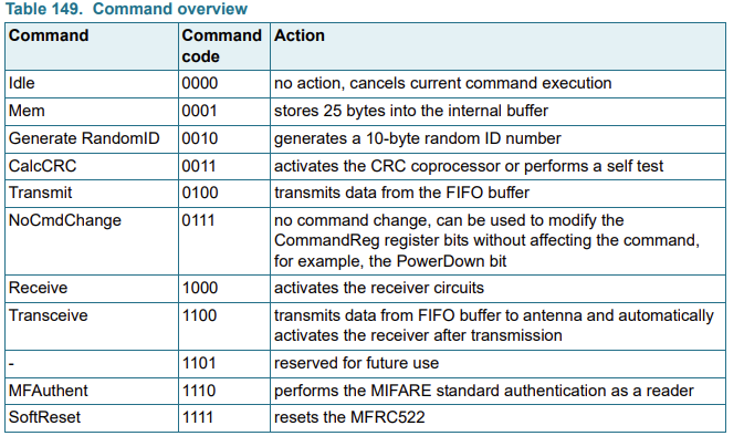
So, it’s like at first, we will configure the FIFO, CRC, Interrupts and timer unit. After that Host MCU will instruct the commands to MFRC522 in order to tell what it has to do. Host MCU will write the command code to the CommandReg Register.
Main commands that would be used are Idle, Transceive, CalcCRC and Transmit commands. Transceive command is the one which has to be sent from Host MCU to MFRC522 to send the FIFO buffer data to the antenna, which is further propagated to the RFID readers. And according to the data which we have written in FIFO RFID readers would act and give response.
Each command that needs a data bit stream (or data byte stream) as an input immediately processes any data in the FIFO buffer. An exception to this rule is the
Transceive command. Using this command, transmission is started with the BitFramingReg register’s StartSend bit.

Above is the simplified block diagram of MFRC522 module. MFRC522 has an internal memory, power supply, interrupt pins, FIFO buffer, Antenna and analog interface, digital module for communicating with Host MCU.
Analog Interface handles the modulation and demodulation of the analog signals. FIFO Buffer ensures fast and convenient data transfer.
Register bank are the set of registers through which MFRC522 would be configured and initialized to use. Parameters like Clock, Interrupts, status of errors while communicating with RFID readers, CRC calculation, FIFO configuration and etc need to be configured before using the MFRC522.

Host MCU will send PCD Commands to MFRC522, according to which it will perform some operations. MCU will send these commands by writing into one of the registers of PCD.( For MFRC522 CommandReg is register)
Operations like:
- Activation of CRC Coprocessor
- Transmission of data from FIFO buffer of MFRC522 and activation of receiver circuits to get the response from PICC
- transfer of data from FIFO to an internal buffer
- soft reset and authentication-based operations
Further MFRC522 will emit the commands for communicating with PICC, here referred to as PICC Commands, according to which operation with PICC takes place, like scanning of PICC, selecting the PICC, reading and writing the data on PICC. MFRC522 emits these commands via electromagnetic induction and electric coupling. ( That is the main working principle behind the RFID technology)
Host MCU to PCD
Host MCU will send the commands to PCD, according to which PCD will perform the operations like activation of FIFO buffer or CRC coprocessor, and transmission of data from FIFO. We will name these commands as MFRC522 Commands sets. Host MCU will send those commands to PCD (here MFRC522) by writing into the CommandReg Register using low level Host Interface write API.
- Idle Command: Places the MFRC522 in Idle mode.
- Mem Command: Transfers the 25 bytes from the FIFO Buffer to the internal buffer. This command is used when, we want to read the data from PICC( As described in ISO-14443-4 doc), as PICC response is always recorded in PCD FIFO.
- Generate RandomID: generates a 10-byte random ID number.
- CalcCRC: Activates the CRC coprocessor or performs a self test.
- Transmit: transmit data from the FIFO buffer
- NoCmdChange: no command change, can be used to modify the CommandRef register bits without affecting the command
- Receive: activates the receiver circuits
- Transceive: Transmit data from the FIFO buffer to antenna and automatically activates the receiver after transmission.
- MFAuthent: performs the MIFARE standard authentication as a reader
- SoftReset: This command performs a reset of the device. The configuration data of the internal buffer remains unchanged. All registers are set to the reset values. This command automatically terminates when finished.
PCD to PICC
Further there are also command set which PCD have to emit to communicate with PICC and enter the PICC into some state machine.

PICC States:
- Power-off State: In the POWER-OFF state, the PICC is not powered by a PCD operating field
- Idle State: In the IDLE state, the PICC is powered. It listens for commands and shall recognize REQA and WUPA commands.
- Ready State: Cascade levels are handled inside this state to get the complete UID. PICC enters the ACTIVE state when it is selected with its complete UID.
- Active State: PICC complies with ISO-14443-4 to accept protocol activation commands (RATS)
- HALT State: In this state PICC only responds to WUPA command.
- Protocol State: PICC behaves according to 1s014443-4 specifications.
We will name these commands as PICC commands. Host MCU will write these PICC command into the PCD FIFO (refer the MFRC522 FIFO section on how to write the data on FIFO). PCD would transmit the FIFO data when it enters the Transceiver state machine (refer above topic).
PCD would transmit these commands via the electromagnetic induction and communicates with PICC via electronic coupling. PCD’s have RF transceivers through which it emits the electromagnetic waves with commands sets encoded in them. PICC have antenna and small circuitry, which gets energized via electromagnetic waves emitted by PCD and then further both PCD and PICC get coupled together to have 2 way wireless communication. How PCD would send commands to PICC and in return how PICC would respond, that is done according to IS014443 protocol. ISO14443 specifies all the frame formats,PICC command and their format , modulation schemes for RFID technology. 
PICC Frame formats:
- Short Frame:
- Standard Frames
PICC Command Set:
- REQA/WUPA Command: This command is send by PCD to scan the valid and IS014443 compatible PICC’s. This command is in short frame format. Host MCU will write this command into the PCD FIFO, from where this command is transmitted and emitted wirelessly. Response to this command is with ATQA. PICC are in Idle state when listening to this command and after successfully transmitting the ATQA response they enter into Ready State. These commands consist of 7 bits, as specified below:

- ANTICOLLISION/SELECT Command: PICC are in ready state when listening to this command and after this command they enter into ACTIVE STATE. This Command is used to get the UID of the scanned PICC and further select the corresponding PICC for Reading and writing data from it. For the MF1S503 PICC’s UID is of 4 bytes, for that only 1 cascade level is needed.
These commands need to be configured and then these bytes are written into The PCD FIFO for transmission and emission of signal to PICC wirelessly. This Command consists of:
- Select code SEL(1byte): Specify the cascade level.
- No of valid bits NVB (1 byte): specify number of bytes that would be transmitted by PCD to PICC (including SEL, NVB and below point)
- 0 to 40 data bits of UID according to value of NVB.

ANTICOLLISION Command consist of:
- Select Code: Cascade level 1= 0x93
- No of valid bits NVB = 0x20

Response to ANTICOLLISION Command is with the UID of the Scanned PICC(0xEA, 0x24, 0x77, 0x15) and its CRC(0xAC).
- SELECT Command consists of:
- Select code: Cascade level 1 = 0x93
- No of valid bits NVB – 0x70
- 0 to 40 data bits of UID that has been received in ANTICOLLISION Command( 0xEA, 0x24, 0x77, 0x15)
- CRCA(1 byte) : CRC of SELECT Command would be calculated by PCD and then it would be sent to PICC. And When PICC receives the SELECT Command it will check this CRCA and then will send the ACK.(0xAC)

Response to SELECT Command is with the Select Acknowledge:


MFRC522 IC has 32 pins in total and it comes in SOT617-1 package.

Pin description can be found from the datasheet of MFRC522. To use the MFRC522 IC its module is widely available and quite inexpensive. Can be brought from Robu at cost of 150 rupees. With the module an RFID tag and a key fob tag of MIFRAME Classic 1KB comes in.

In MFRC522 module, IC has 8 pins exposed out for connection and connecting to host MCU.
- The module has 4 pins exposed out for connecting it to host MCU using either SPI, I2C or UART. By default, reader can communicate with a microcontroller over a 4-pin SPI with a maximum data rate of 10 Mbps. It also supports I2C and UART protocols. As told in MFRC522 functional description part, MFRC522 checks the host interface type automatically depending on the signals on it’s control pins.
- MFRC522 module has 1 interrupt pin also exposed out, which can be used to trigger interrupts to alert the microcontroller when a RFID tag is in the vicinity.
- And remaining 3 pins are power supply pins and a reset pin. Reset pin is used for power down mode and reset signal. Module requires the power supply of 3.3 V, that is provided via VCC and GND pins.


STM32F103 & ADC: Single Channel Conversion
In the last post, we have gotten to know about the features of ADC Peripheral that we have in STM32
UART(Universal Asynchronous Receiver Transmitter) Explained!
Explore this blog to explore basics of UART Communication protocol in Semiconductor Chip world
GPIO Control over S32K144(MCAL Driver)
Interfacing LEDS and Switches via Port Driver of Autosar MCAL Layer using ElecronicsV3 Board(S32K144 MCU)

FRDM i.MX93 Demystified: The Hardware That Makes AI Work at the Edge
Imagine you’re handed a powerful little board, no bigger than your palm. At first glance, it looks like a jungle
Hardware Security Module peripheral for Automotive Chips
Learn About Advance Cryptography Peripheral in Microcontrollers: The HSM Peripheral (Hardware Security Module)

UART Peripheral in S32K144 MCU
LPUART Peripheral in S32K144 MCU || Briefing about LPUART Peripheral in S32K1xx MCU’s