Over 10 years we help companies reach their financial and branding goals. Engitech is a values-driven technology agency dedicated.

Gallery

Contacts

411 University St, Seattle, USA

engitech@oceanthemes.net

+1 -800-456-478-23

Display Screens Sensors and Modules Tech

What is OLED Technology?

OVERVIEW

Nowadays we see oled display being used everywhere be it the phones , TVs , laptops or PCs , smartwatches . They sure are better than old chunky CRT TV displays that were bulky and didn’t deliver the desired picture quality , with the introduction of the LCD and backlight LEDs the things sure got better with the chunkiness of the display gone but the picture quality still wasn’t what one desired of but with the release of the OLED display all these problems became a thing of past. OLED or organic light emitting diode were invented in 1987 by Ching Tang and Steven Van Slyke from Kodak but it was until 2004 when SONY released a OLED TV. In fact in CES 2019 , there were some innovative inventions that were released in the OLED domain with the companies trying to come up with foldable display and some exceptional picture quality.

TYPES OF OLED

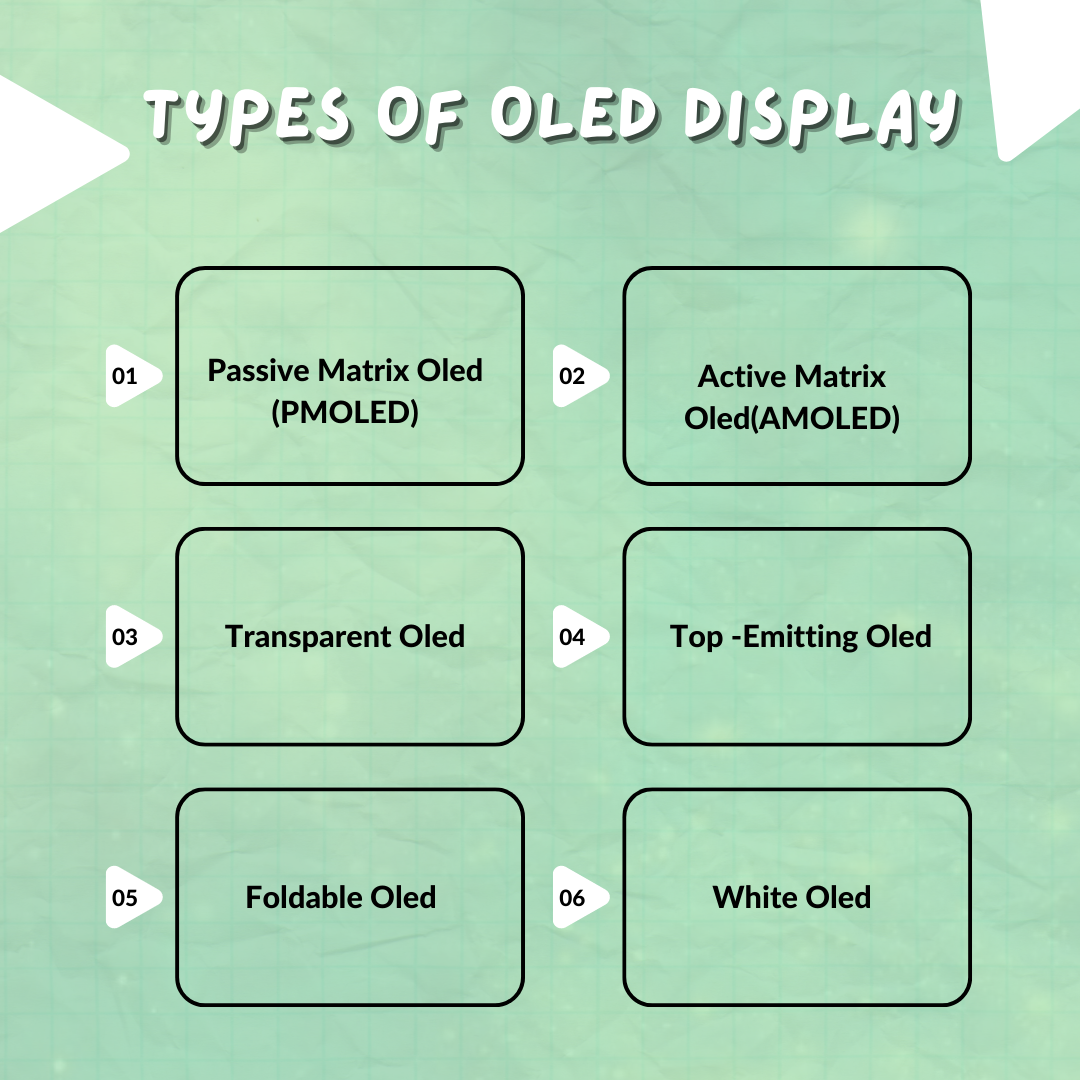
Passive Matrix Oled (PMOLED)

Pmoleds have strips of cathode , anode and organic layer. The anode strips are perpendicular to cathode strips it is their intersection that makes a pixel . External circuitry applies current to the cathode and anode strips to decide which pixel to light up. They are used in MP3 players , cell phones etc.


Active Matrix Oled(AMOLED)

Amoleds have full layer of anode and cathode and organic molecules . The anode layer overlaps the TFT matrix array . The TFT array is the matrix circuitry that decides which pixel gets turned on form the image. Since they consume less electricity they are used in TV screens , BillBoards, Computer Monitors.


Transparent Oled

A Transparent Oled has all the components cathode, anode, substrate transparent and when off the display is 85 percent transparent. When switched ON the display allows the transfer of light in both the directions.


Top Emitting Oled

The Top Emitting Oled is have substrate that is either opaque or transparent . They are best suited for active matrix design . They are used in smartcards


Foldable Oled

They are substrate that made of flexible metallic foil , plastic . They are durable and are easier to replace in case of damage . They are used in smart clothing , GPS receivers , IC computers.


White Oled

They are made of white light that is more uniform and energy efficient rather than fluorescent lights. They posses true color of incandescent lights 

BESIDES THESE OLEDS ARE ALSO CATEGORIZED ON THE BASIS OF

  • Monochrome Blue
  • Monochrome white
  • Yellow Colour
  • 3 Pins (supports only I2C)
  • 7 Pins(supports both I2C and SPI)
  •    SSD1306
  •     SSD1331
  • 0.91 inch(128×32)
  • 0.96 inch(128×64)

HOW OLEDs WORKS

FIG -1 SIZE OF A SINGLE PIXEL

FIG-2 RGB COLOR FILTERS INSIDE A PIXEL

FIG -3 CONVERTING EACH COLOR INTO BINARY

FIG -4 CROSS SECTION VIEW OF OLED

FIG-5 CHANGING THE ORIENTATION OF THE POLARIZER TO GENERATE DIFFERENT COLORS

FIG -6 ELECTRON HOLE PAIR COMBINATION TO GENERATE LIGHT

FIG – 7 DOPING OF SUBSTRATE TO GENERATE LIGHT OF VARIOUS WAVELENGTH

USE CASES OF OLED DISPLAY


HOW TO CONNECT THE DISPLAY WITH THE MICROCONTROLLER

WE WILL BE COVERING THE DETAILS ON HOW TO CREATE AN EMBEDDED DRIVER FOR THE DISPLAY IN THE NEXT BLOG . IN THIS WE’LL BE COVERING A BRIEF OVERVIEW OF THE 2 METHODS THAT CAN BE USED TO COMMUNICATE WITH THE DISPLAY.

Tigger MUX Control(TRGMUX) Peripheral in S32K144 MCU

What is TRGMUX peripheral? TRGMUC provides an extremely flexible mechanism for connecting various trigger sources to multiple pins/peripherals. The trigger multiplexer (TRGMUX) module allows software to configure the trigger inputs for various peripherals.   The TRGMUX module allows software to select the trigger source for peripherals.   TRGMUX is a peripheral which provides mechanisms for connecting various trigger sources to multiple pins/peripherals. Each peripheral that accepts external triggers usually has one specific 32-bit trigger control register. Each control register supports upto 4 triggers and each trigger can be selected from available trigger sources.   Author: Kunal Gupta

Read More »

PDB (Programmable Delay Block) Peripheral in automotive microcontroller (NXP S32K144)

What is Programmable Delay Block(PDB) peripheral? PDB provides controllable delays from either an internal or an external trigger, or a programmable interval tick, to the hardware trigger inputs of ADCs. PDB can also provide pulse outputs that are used as the sample window in the CMP block.   The PDB contains a counter whose output is compared to several different digital values. If the PDB is enabled, then a trigger input event will reset the PDB counter and make it start to count. A trigger input event is defined as a rising edge being detected on a selected trigger input source, or if a software trigger is selected and the Software Trigger bit (SC[SWTRIG]) is written with 1 Author: Kunal Gupta

Read More »
CAN Bit TIming

CAN Bit Timing Explained

Bit timing in CAN is all about ensuring that every node on the network can correctly interpret the bits being transmitted. This synchronization is crucial for maintaining the integrity and efficiency of data communication. Bit Segmentation Each bit in a CAN frame is divided into several segments: Synchronization Segment (Sync_Seg): This is the part where the actual synchronization occurs. It’s always one-time quantum (TQ) long and helps align the clocks of all nodes on the network. Propagation Segment (Prop_Seg): This segment compensates for the physical delay in signal propagation across the network. Phase Segment 1 (Phase_Seg1): This is used to compensate for edge phase errors by lengthening the bit time if necessary. Phase Segment 2 (Phase_Seg2): Similar to Phase_Seg1, but it shortens the bit time if necessary. Each of these segments is made up of a certain number of time quanta (TQ), which are the smallest time units in a CAN network. Sample Point The sample point is a critical point within the bit where the bus level is read and interpreted as a logical value. Here’s why it’s so important: Accurate Bit Reading: The sample point is where the CAN controller reads the bit value. It is crucial to set the sample point accurately to minimize errors due to signal noise or other disturbances on the bus. Preferred Value: Typically set at 87.5% of the bit time, this value is preferred by protocols like CANopen and DeviceNet. This means that the bit is sampled after 87.5% of its duration has passed. Adjustable Range: The sample point can vary from 50% to 90% of the bit time, allowing flexibility depending on the network requirements and conditions. For example, ARINC 825 uses a default value of 75%. Noise Minimization: Setting the sample point correctly helps in minimizing the impact of signal noise. Sampling too early or too late can lead to incorrect bit interpretation, especially in noisy environments. Understanding Bit Rate and Bit Timing Bit Rate The bit rate in CAN communication refers to the speed at which data is transmitted over the CAN bus, typically measured in bits per second (bps). The bit rate is a crucial parameter because it determines how quickly data can be sent and received between nodes on the network. Common bit rates in CAN systems include 125 kbps, 250 kbps, and 500 kbps, with some systems operating at even higher speeds, such as 1 Mbps. Bit Timing Bit timing in CAN communication is the precise control of the duration and positioning of each bit transmitted on the bus. Proper bit timing ensures that all nodes on the network sample the bits at the same point, leading to accurate and synchronized data transmission. Bit timing is divided into several segments within each bit time, which collectively ensure robust and reliable communication. How Bit Timing Ensures Synchronization To maintain synchronization, the CAN controller can adjust the length of a bit by an integral number of time quanta (TQ). The maximum value of these adjustments is termed the Synchronization Jump Width (SJW). Hard Synchronization: Occurs on the recessive-to-dominant transition of the start bit. The bit time is restarted from this edge. Resynchronization: Occurs when a bit edge doesn’t occur within the Sync_Seg in a message. One of the Phase Segments is shortened or lengthened, depending on the phase error, up to the SJW. Factors Affecting Bit Rate Four primary factors influence the CAN bit rate: Oscillator Tolerance: Variations in the oscillator frequency can affect the timing accuracy. High-precision oscillators are essential for maintaining a stable bit rate. Propagation Delay: The physical length and quality of the CAN bus can introduce delays. Prop_Seg is adjusted to compensate for these delays. Network Load: Heavy network traffic can lead to delays and timing issues. Proper network design and bit timing configuration help mitigate these problems. Bus Length: Longer bus lengths introduce more propagation delay, requiring adjustments in the Prop_Seg to maintain synchronization. Prescaler Division The prescaler is used to divide the clock frequency to generate the required clock frequency for CAN. For example, if the clock frequency is 48 MHz and we need an 8MHz CAN clock, the prescaler value would be 6. How the Prescaler Division Works Clock Frequency: The original clock frequency provided by the oscillator. Prescaler Value: The value by which the original clock frequency is divided to achieve the desired CAN Clock Frequency. IMPORTANT The CAN system clock is chosen so that the desired CAN bus Nominal Bit Time (NBT) is an integer number of time quanta (CAN system clock periods) from 8 to 25. Time Quanta Definition: The time quantum (tQ) is the basic time unit in CAN bit timing. It is derived from the CAN system clock divided by the prescaler. Calculation: For example, if the CAN system clock is 48 MHz and the prescaler is set to 6, then: Nominal Bit Time (NBT) Definition: The Nominal Bit Time (NBT) is the total duration of a single CAN bit, measured in time quanta (tQ). It is the sum of the time segments within a bit period: Sync_Seg, Prop_Seg, Phase_Seg1, and Phase_Seg2. Components: Sync_Seg: The synchronization segment, always 1 tQ. Prop_Seg: The propagation delay segment, compensates for the signal propagation delay. Phase_Seg1: The first phase segment, can be adjusted to resynchronize the clock. Phase_Seg2: The second phase segment, also adjustable for resynchronization. Calculation: Practical Example of Bit Timing Calculation For calculating Bit Time and Segmentation, some important parameters are taken into account before starting the calculation. Parameters: Bit rate MCU Clock/Oscillator Frequency Bus length Bus propagation delay Propagation delay of TxD plus RxD offered by CAN Transceiver But, usually, values like total propagation delay offered by CAN transceiver, Bus length, and Bus propagation delay, are pre-defined values in their hardware datasheet. Question: Conclusion Understanding CAN bit timing and how the bit rate is adjusted is crucial for ensuring reliable communication in a CAN network. By properly configuring the timing parameters and taking into account factors like oscillator tolerance, propagation delay, network load, and bus length,

Read More »
Kunal Gupta
Author: Kunal Gupta

Author

Kunal Gupta

Leave a comment

Stay Updated With Us

Error: Contact form not found.

      Blog