

LPUART Peripheral in S32K144 MCU || Briefing about LPUART Peripheral in S32K1xx MCU’s
Table of Contents About GPIO Peripheral The pins which can be configured by the software at runtime to perform various functions are called GENERAL-PURPOSE INPUT/OUTPUT (GPIO) pins. With the help of software one can program the GPIO pins mainly as: Digital Output It compares the external voltage signal with a predefined threshold. Digital Input It controls the Voltage of the pin Analog Function It performs ADC (Analog to Digital Conversion) or DAC (Digital to Analog Conversion) Other Functions or Alternate Functions It makes the pin to perform other functions like PWM output, timer-based captures, external interrupts, and various other interfaces like SPI, I2C, UART communications. Before coming to the Schmitt Trigger Understanding, have a quick recap of Pull Up, Pull Down and Open Drain Configurations from MPU6050 Implementation blog Implementation of MPU6050 with STM32 – gettobyte GPIO Input: Schmitt Trigger GPIO Output Speed Slew Rate GPIO Input: Schmitt Trigger A SCHMITT TRIGGER is a device which uses a voltage comparator to convert a noisy or slow signal edge into a clean and desirable edge instantaneously. For a real time system, the external signals do not change instantly, due to slower slew rate which depends on inheritance parasitic capacitance, resistance or an inductor at the input side. As the processor chip has a Schmitt Trigger, it increases the slew rate and increases the noise immunity for the signals which are captured. Let us understand the implementation of the Schmitt Trigger. It consists of a voltage comparator with positive feedback. The output Vout depends between two input voltage V+ and V–. If V+ > V–, Vout is quickly saturated to VSAT, otherwise Vout = 0 For an ideal op-amp, the current flowing through resistor R3 is zero and thus we have Vref = V– The op-amp output Vout has two saturation values, as shown below Vout = VSAT if V– <V+ 0 if V– < V+ However, V+ depends on Vout and Vin· Therefore, Vout depends on both the input Vin and the recent history of Vout· Such an effect is called hysteresis. Using KCL, assuming that the current flow in the non inverting input terminal of op-amp is zero, Vin – V+ /R2 = V+ – Vout / R1 On solving the above equation we will get, Vin = R2Vout + R1Vin / R1 + R2 At the time instant when Vout transits from one saturation value to the other saturation value, we have V+ = Vref Thus, Vref = R2Vout + R1Vin / R1 + R2 Solving further we get, Vin = (1 + R2/ R1)Vref – (R2/R1)Vout As discussed earlier, Vout has only two possible values. If Vout = 0 initially and Vin increases, we can obtain the trigger high threshold VTH at which Vout transits to VSAT: VTH = (1 + R2/R1) Vref – (R2/R1)*0 = (1 + R2/R1)Vref On the other hand, if Vout = VSAT initially and Vin decreases, we can obtain the trigger low threshold VTL at which Vout transits to 0: VTL = (1 + R2/R1) Vref – (R2/R1)VSAT Vout can be determined by comparing it with two thresholds VTH and VTL. When Vin climbs through VTH , Vout is rapidly switched to the upper limit VSAT· Conversely, once Vin falls below VTL, Vout makes a transition to the lower limit. Note that VTH > VTL , i.e., the threshold for switching to high is greater than the threshold of switching to low. A Schmitt trigger when compared, Provide a better boise rejection. Larger threshold for switching high and low for switching. Immune to undesired noise. GPIO Output Speed Slew Rate The SLEW RATE of a GPIO pin is the speed of change of output voltage with respect to unit time. Slew Rate = ΔV/ Δt In simple words, If the GPIO pin changes from LOGIC LEVEL 0 to LOGIC LEVEL 1, the voltage changes from 0V to 5V in just 5µs, then the slew rate is simply 1V/µs. The higher the slew rate, the shorter time the output voltage takes to rise or fall to desired values. Therefore, a higher slew rate allows faster speed at which the processor can toggle the logic level of a GPIO pin. A shorter rise and fall time allows a GPIO pin to change its logic value more rapidly. A high slew rate can result in significant electromagnetic interference (EMI), also known as radio frequency interference (RFI), to nearby electronic circuits. This is due to the large-amplitude and high-frequency harmonics produced by a fast-rising and falling signal, which can cause malfunctions in a victim circuit through radiation, conduction, or induction. To reduce EMI disturbance, a slower slew rate is generally preferred. GPIO IN STM32WB Each GPIO port has 4 32-bit Configuration Registers (GPIOx_MODER, GPIOx_OTYPER, GPIOx_OSPEEDR and GPIOx_PUPDR) 2 32-bit Data Register (GPIOx_IDR and GPIOx_ODR) A 32-bit Set/Reset Register (GPIOx_BSRR) A 32-bit locking Register (GPIOx_LCKR0 and 2 32-bit Alternate Function Select Register (GPIOX_AFHR and GPIOX_AFLR) Main feature sog GPIO are Output states: push-pull or open drain + pull-up/down Speed selection for each I/O Input states: floating, pull-up/down, analog Fast toggle capable of changing every two clock cycles Highly flexible pin multiplexing allows the use of I/O pins as GPIOs or as one of several peripheral functions GPIO Functional Description The port bit of GPIO can be configured by the software depending upon the hardware characteristics in various modes such as: Input floating Input pull-up Input-pull-down Analog Output open-drain with pull-up or pull-down capability Output push-pull with pull-up or pull-down capability Alternate function push-pull with pull-up or pull-down capability Alternate function open-drain with pull-up or pull-down capability Each I/O port bit is freely programmable, however the I/O port registers have to be accessed as 32-bit words, half-words or bytes. The purpose of the GPIOx_BSRR register is to allow atomic read/modify access to any of the GPIOx_ODR registers. In this way, there is no risk of an IRQ occurring between the read and the modify access. The above diagram shows the basic structure of a
Table of Contents About STMicroelectronics STMicroelectronics is a leading provider of semiconductor solutions that are seamlessly integrated into billions of electronic devices used by people worldwide on a daily basis. The semiconductor company builds products, solutions, and ecosystems that enable smarter mobility, more efficient power and energy management, and the wide-scale deployment of the Internet of Things and connectivity technologies. To know more about STMicroelectronics refer to its website: www.st.com. Going back in history, ST was formed in 1987 by the merger of two government-owned semiconductor companies: Italian SGS Microelettronica (where SGS stands for Società Generale Semiconduttori, “Semiconductors’ General Company”), and French Thomson Semiconductors, the semiconductor arm of Thomson. In this blog, we are going to start with ST IoT-based Nucleo Board STm32WB55. What is STM32WB Series all about? The STM32WB55xx and STM32WB35xx are advanced multiprotocol wireless devices that boast ultra-low-power consumption. These devices are equipped with a powerful and efficient radio that is compliant with the Bluetooth® Low Energy SIG specification 5 and IEEE 802.15.4-2011 (Zigbee). Additionally, they feature a dedicated Arm® Cortex®-M0+ processor that handles all real-time low-layer operations. These cutting-edge devices are perfect for a wide range of applications that require reliable and efficient wireless communication. Whether you’re working on a smart home project, a wearable device, or an industrial automation system, the STM32WB55xx and STM32WB35xx are the ideal choices. With their advanced features and capabilities, these devices are sure to revolutionize the way we think about wireless communication. So why wait? Start exploring the possibilities today and discover what the STM32WB55xx and STM32WB35xx can do for you! The devices have been meticulously crafted to operate on minimal power and are built around the high-performance Arm® Cortex®-M4 32-bit RISC core, which can operate at a frequency of up to 64 MHz. This core boasts a Floating-point unit (FPU) single precision that supports all Arm® single-precision data-processing instructions and data types. Additionally, it is equipped with a full set of DSP instructions and a memory protection unit (MPU) that enhances application security. These devices have been designed with the utmost care and attention to detail, ensuring that they are not only efficient but also highly effective. The Arm® Cortex®-M4 32-bit RISC core is a powerful tool that enables these devices to perform at an exceptional level, while the FPU single precision and DSP instructions provide unparalleled accuracy and precision. Furthermore, the memory protection unit (MPU) ensures that your applications are secure and protected from any potential threats. Enhanced inter-processor communication is provided by the IPCC with six bidirectional channels. The HSEM provides hardware semaphores used to share common resources between the two processors. The devices embed high-speed memories (up to 1 Mbyte of flash memory for STM32WB55xx, up to 512 Kbytes for STM32WB35xx, up to 256 Kbytes of SRAM for STM32WB55xx, 96 Kbytes for STM32WB35xx), a Quad-SPI flash memory interface (available on all packages) and an extensive range of enhanced I/Os and peripherals.  About STM32WB55 Architecture Memories Security and Safety True random number generator (RNG) RF Subsystem Low Power Modes Clocks and Startup General Purpose Input Output(GPIOs) Direct Memory Access (DMA) Interrupts and Events Analog to Digital Convertor (ADC) Comparators (COMP) Touch Sensing Controller Liquid crystal display controller (LCD) Timers and watchdogs Real-time clock (RTC) and backup registers Inter Integrated Circuit (I2C) Universal Synchronous/Asynchronous Receiver Transmitter (USART) Serial Peripheral Interface(SPI) Serial audio interfaces (SAI) Quad-SPI memory interface (QUADSPI) Architecture Architecture STM32WB55 Architecture The host application is housed on an Arm® Cortex®-M4 CPU (named CPU1) that connects with a generic microcontroller subsystem. The RF subsystem is made up of a specialized Arm® Cortex®-M0+ microprocessor (named CPU2), Bluetooth Low Energy and 802.15.4 digital MAC blocks, an RF analog front end, and proprietary peripherals. All Bluetooth Low Energy and 802.15.4 low-layer stack functions are handled by the RF subsystem, which limits communication with the CPU1 to high-level exchanges. Some functions are shared between the RF subsystem CPU (CPU2) and the Host CPU (CPU1): Flash memories SRAM1, SRAM2a, and SRAM2b (SRAM2a can be retained in Standby mode) Security peripherals (RNG, AES1, PKA) Clock RCC Power control (PWR) Memories Memories STM32WB55 Memories 2.1. Adaptive real-time memory accelerator (ART Accelerator) The ART Accelerator is a memory accelerator optimized for STM32 industry-standard Arm® Cortex®-M4 processors. It balances the inherent performance advantage of the Arm® Cortex®-M4 over flash memory technologies. To release the processor near 80 DMIPS performance at 64 MHz, the accelerator implements an instruction prefetch queue and branch cache, which increases program execution speed from the 64-bit flash memory. Based on CoreMark benchmark, the performance achieved thanks to the ART accelerator is equivalent to 0 wait state program execution from flash memory at a CPU frequency up to 64 MHz. 2.2. Memory protection unit In order to prevent one task from unintentionally corrupting the memory or resources used by any other active task, the memory protection unit (MPU) is used to manage the CPU1’s accesses to memory. This memory area is organized into up to eight protected areas. The MPU is especially helpful for applications where some critical or certified code must be protected against the misbehavior of other tasks. It is usually managed by an RTOS (real-time operating system). 2.3. Embedded flash memory The STM32WB55xx and STM32WB35xx devices feature, respectively, up to 1 Mbyte and 512 Kbytes of embedded flash memory available for storing programs and data, as well as some customer keys. 2.4. Embedded SRAM The STM32WB55xx devices feature up to 256 Kbytes of embedded SRAM, split in three blocks: SRAM1: up to 192 Kbytes mapped at address 0x2000 0000 SRAM2a: 32 Kbytes located at address 0x2003 0000 also mirrored at 0x1000 0000, with hardware parity check (this SRAM can be retained in Standby mode) SRAM2b: 32 Kbytes located at address 0x2003 8000 (contiguous with SRAM2a) and mirrored at 0x1000 8000 with hardware parity check. Security and Safety Security and Safety The STM32WB55xx contain many security blocks both for the Bluetooth Low Energy or IEEE 802.15.4 and the Host application. It includes: Customer storage of the Bluetooth Low Energy and
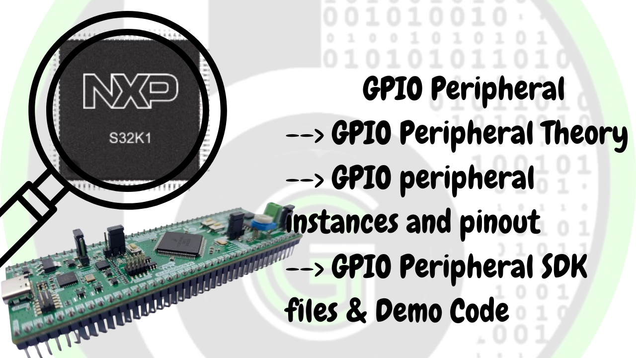
What is GPIO peripheral in NXP S32K1xx MCU || Briefing about how to use GPIO peripheral in NXP S32K1xx MCU’s
Decoding the working of MFRC522 RFID Receivers to interface them with Host MCU/MPU
In the last blog I talked about the basics of MPU6050, this time let’s see how to interface it with the STM32 based controller and get the values of accelerometer and Gyro sensor. But before starting first, let’s see the I2C block and the STM32 I2C block to get some idea of the basic structure of the I2C protocol. Figure 1: I2C Hardware Circuit The above circuit diagram shows the hardware connection of the I2C protocol in open drain configuration. The external pull up resistors are being used to make the circuit work efficiently. These days the controllers come with the internal pull up resistors so while writing the code for the same these resistors can be pulled up in the configuration. Before proceeding further lets understand certain terms like pull up, pull down, open drain etc. While using an I/O pin, in the digital domain it has values as LOGIC 1 (HIGH), LOGIC 0 (LOW) and Z-STATE (HIGH IMPEDANCE or FLOATING or TRI-STATE). The purpose of pull up and pull down is to maintain these states of the pin while working. PULL-UP means that the pin is internally connected to the power supply via a resistor and is read as LOGIC 1. PULL-DOWN means that the pin is internally connected to the ground via a resistor and is read as LOGIC 0. In between the two in the configuration, when the pin is neither pull-up nor pull-down and the analog value cannot be represented in the logic value, this state is termed as Z-STATE where there is a floating value. Figure 2: Pull-up and Pull-Down Configuration Now let’s understand the Push-Pull and Open Drain configurations. PUSH-PULL Configuration: This configuration consist of a pair of complementary transistors which works as: For LOGIC 0, the transistor connected to the ground is turned on to sink an electric current from the external circuit. For LOGIC 1, the transistor connected to the power supply is turned on, and it provides an electric current to the external circuit connected to the output pin. The slave address of the MPU-6050 id 0b110100x, a 7-bit long. Here the LSB bit i.e.x in the 7-bit long address is determined by the logic level at AD0 pin.If x=0 i.e., pin AD0 is Logic LOW otherwise Logic HIGH. Figure 3: Push-Pull Configuration Figure 4: The Logic 0 and 1 for Push-Pull Configuration OPEN-DRAIN Configuration: This configuration consist of a single transistors which works as: For LOGIC 0, the transistor connected to the ground is turned on to sink an electric current from the external circuit. For LOGIC 1, it cannot supply any electric current to the external load because the output pin is floating, connected to neither the power supply nor the ground. Hence the Open-Drain has two states LOGIC 0 (LOW) and LOGIC 1 (Z-STATE). This configuration use external pull up resistor. Figure 5: Open-Drain Configuration Figure 6: The Logic 0 and 1 for Open-Drain Configuration I2C Let’s analyze the functional block diagram of the STM32. As shown in the figure, the I2C protocol consists of SDA and SCL lines along with an additional pin SMBA used in SMB protocol known as System Management Bus. The figure shows that there is a single Data Register along with the single Shift Register as the protocol is half -duplex. The address block is also there and a comparator to compare the addresses. The control logic consists of Control Register (CR 1 and CR2) and Status Registers (SR1 and SR2) along with the Clock Control Register for generating the clock for the communication. Figure 7: I2C Block Diagram I2C Implementation Of Figure 9: Pin Connections Above is the pin connection of the MPU6050 with the STM32F411CE. Now set up the stm32 environment as follows: Step 1 Step 2 Step 1 Set up the RCC ad the SYS in the STM32Cube IDE as shown: Step 2 Now enable the I2C1 in the standard mode. Now starting with the code create a mpu6050.h file in the Inc folder and mpu6050.c file in Scr folder. We are all done. Let’s start with the code. In total there are around 80 registers in the IC but during the code all the registers are not required there are certain sets of registers which we are going to use which we will be defining in the header file mpu6050.h. These registers are: Name of the Register Address of the Register (Hex) Function REG_MPU6050_ADDR 0xD0 It is the device address for the MPU6050 module REG_SMPLRT_DIV 0x19 This register specifies the divider from the gyroscope output rate used to generate the Sample Rate for the MPU-6050. REG_GYRO_CONFIG 0x1B This register is used to trigger gyroscope self-test and configure the gyroscopes’ full scale range. REG_ACCEL_CONFIG 0x1C This register is used to trigger the accelerometer self test and configure the accelerometer full scale range. This register also configures the Digital High Pass Filter (DHPF). REG_ACCEL_XOUT_H 0x3B These registers store the most recent accelerometer measurements. REG_TEMP_OUT_H 0x41 These registers store the most recent temperature sensor measurement. REG_GYRO_XOUT_H 0x43 These registers store the most recent gyroscope measurements. REG_PWR_MGMT_1 0x6B This register allows the user to configure the power mode and clock source. It also provides a bit for resetting the entire device, and a bit for disabling the temperature sensor. REG_WHO_AM_I 0x75 This register is used to verify the identity of the device. The contents of WHO_AM_I are the upper 6 bits of the MPU-60X0’s 7-bit I2C address. The least significant bit of the MPU-60X0’s I2C address is determined by the value of the AD0 pin. The value of the AD0 pin is not reflected in this register. Apart from these registers we have two structures and the function definitions that we are using in the main file. Lets now jump directly towards the mpu6050.c file and see how things are working. In this phase, keep in mind the 3 things. Initializing the mpu6050. Read the RAW values of accelerometer and gyroscope Convert the RAR values to ‘g’ and ‘dps’ for Accelerometer
What is PWM? PWM or Pulse Width Modulation, is a type of digital electrical signal which is periodic in nature, with a rectangular waveform. There are certain terms associated with PWM which we need to understand before we move ahead. Here’s a graphical representation of a PWM signal- · ‘Period’ = Tp , is the time it takes to repeat the same waveform · ‘Duty cycle’ is the time for which the signal is a logic 1 by the total time period. Ton is the time for which the pulse is high Hence, Duty cycle % = (Ton/ Tp) X 100 · ‘Frequency’ = F is the number of times the waveform repeats in a second. So, F = 1/Tp. Applications of PWM signals PWM signals have an extremely wide range of applications, here are a few of them- · Variable voltage generator– if you vary the duty cycle of a PWM signal and apply it to certain electrical components, the components act as if they are receiving analog signals. This is because the response time of the components is finite. So, components like LEDs, buzzers, brushed DC motors etc. can be controlled by PWM signals. Meaning, you could control speed of a motor, brightness of an LED or amplitude of a buzzer and so on. The voltage that they receive has a linear relationship with the duty cycle. So, if logic 1 is 5 Volts 0% duty cycle – 0V 25% duty cycle – 1.25 V 50% duty cycle – 2.5 V 75% duty cycle – 3.75V 100% duty cycle – 5V · As a control signal – Some electrical devices/components analyze PWM signals that they are receiving to give a corresponding output. So, changes in the duty cycle are reflected in the output. These include Servo motors, electronic speed controllers (ESCs) and many more. Here, the devices respond only to specific PWM duty cycles and frequencies If you take the example of servo motors, they can only be operated at 50Hz signal with a duty cycle of 2.5 % to 12% . Anything beyond that doesn’t result in the movement of the servo. (The frequency and duty cycles vary from among different servos, this is a very common value which most 180-degree servos respond to) Similarly, ESCs respond to a PWM signal with ON time of 1ms for minimum throttle and 2ms for maximum throttle with PWM frequency of 50 Hz. Some devices such as HCSR04 ultrasonic sensors give an output as a PWM signal in which the pulse width corresponds to the time it took for the ultrasonic wave to be received. How is PWM signal Generated on STM32?? Timer peripheral STM32 blue pill has 15 pins which can generate a PWM signal, with other models having even more pins for PWM generation. In this section, we will try to understand how PWM signals are generated by STM32 Every microcontroller has a built-in circuit which can measure the passing of time. These are called Timers. What timers essentially do is count up to a certain number and upon reaching that number, they change the value of a certain register to indicate that the timer has counted up to that number. Now, the time it takes to increment this count by 1 is determined by the timer’s clock frequency. So, if the frequency of a timer is 1KHz, its time period will be 1 Millisecond. Hence, if we count up to 10, we have measured the passing of 10 Milliseconds. This is how, by simply incrementing a number, timers can measure the time that has passed since the timer began counting. (This is how the HAL_Delay() function generates delays) The maximum count a timer can make is determined by its register size. So, an 8 bit timer can count up to 28 = 256, 10-bit timer –210 = 1024 16-bit timer –216 = 65536 32-bit timer –232 = 4294967296 So, a 1 bit increase in timer size equals to double the count Timers are extremely necessary for the functioning of a microcontroller as a lot of events in programs are time based, which you may not even realize. Timer Peripheral modes and features Coming to STM32 Blue pill, it has 4 timers of 16-bit size. To perform these functions, they need to be in specific modes. Here are all the modes in which timers can operate in STM32- 1. Input capture mode– In this mode, a pin on the board is set as input on which a PWM signal is sent by some device and we measure the frequency and duty cycle of that signal. This can be used to interface with devices such as HCSR04 ultrasonic sensors, which send a PWM signal as input to the microcontroller, where different parameters of PWM signals can be used to determine the distance which the sensor is trying to measure. 2. Output compare mode– In this mode, the timer is used as a counter and the count is compared to a register which contains a pre-programmed value, when they are equal, a software interrupt is generated and using this, a given pin is switched high or low. This mode comes in very handy when you are making a project which requires you to use multiple peripherals and at the same time generate a rectangular waveform of a given frequency and duty cycle, as it is interrupt based. 3. One pulse mode– In this mode, a pulse can be generated based upon a trigger from an input pin on the board , the pulse generation takes place after a certain delay from when the input trigger pulse was detected. This can be considered as a combination of mode 1&2 (IC &OC) 4. PWM generation mode– In this mode, we can generate a PWM signal on a given pin by fixing a frequency and a duty cycle. This is the mode we will be using to generate PWM signals through the main loop. The difference of this mode to mode 2 (Output compare
What is STM32 ? STM32 is a family of 32-bit Microcontrollers and development boards manufactured by ST Microelectronics which offer very high performance for a relatively low price. All STM32 microcontrollers are based on ARM Cortex-M processor which make them much better in terms of computing power than most of the common microcontrollers/microcontroller development boards which are available in the market. These microcontrollers also have been provided with software support by ST for developers for free. If you have experience with microcontrollers like Arduino, this is a great step forward in understanding microcontrollers in depth. The STM32 framework allows you to control all peripherals and allows you to tweak them as per your wish, whereas in Arduino IDE, when you program in C++, it comes with in-built functions and libraries which don’t allow you to understand the backend working behind everything. This is very crucial, as it allows you to use the microcontroller to its full potential. STM32 FAMILY The STM32 family of microcontrollers is vast and expansive, offering a variety of options for the consumer to choose from. The family of microcontrollers is broadly classified into 4 categories- High performance ST offers a series of microcontrollers which have the fastest code execution time, high speed data transfer and relatively higher flash memory. Along with this, the feature the most advance peripherals that ST offers. This makes these controllers very useful for real-time applications such as running an RTOS. STM32H7x The H7 series controllers are based on the ARM Cortex M7 offering very high speeds of upto 550Mhz. The microcontroller series comes in two variants, single core and dual core. Dual core H7 series controllers come with an ARM Cortex M4 core as well as an ARM Cortex M7 core which allows for processing work distribution, very useful for applications requiring many peripherals where response time is critical. The dual Core variants also come with an inbuilt SMPS as well. The single core series comes with an ARM Cortex M7 core with clock speed between 220-550Mhz, depending upon the variant. STM32F7x The F7 series controllers are based on the ARM Cortex M7, Thanks to an L1 (level 1) cache, the series delivers the maximum possible theoretical performance of the Cortex-M7 core. Cache memory temporarily stores instructions frequently accessed by the processor STM32F4x – The F4 series is based on the ARM Cortex M4. These controllers have less processing power then H7 and F7 series but still come with advanced peripherals and high flash memory. A very useful line of microcontrollers which offer a wide variety of features and come at a relatively lower cost than that of an F7/H7 controllers. The F4 series is broadly divided into 3 segments- 1.F4 Advance line- Offers up to 180Mhz of clock speed and a maximum of 2 Mb of dual bank flash memory, with advanced peripherals, consisting of communication buses such as QSPI. 2.F4 foundation line- Offer lower flash memory (between 512Kb-1Mb) , with few controllers offering advance peripherals and features such as camera interface and Ethernet MAC. 3.F4 Access line- This line of F4 controllers consists of entry level controller which can be termed ‘High Performance’. These controllers come with lower clock speeds, lower RAM but feature very good power efficiency, while also not compromising on peripherals. Wireless The main focus of the STM32Wx microcontroller family is wireless connectivity. They cover sub-GHz as well as 2.4Ghz frequency range operation The STM32 wireless MCUs are further divided into 2 categories– STM32WB These MCUs have a dual core processor unit, Cortex M4 & Cortex M0+, which allows for processing distribution, making it a great candidate for real-time processing and execution. The MCU series is based on STM32L4 architecture, which offers dynamic voltage scaling, reducing the power consumption of the device. They also support BLE 5.3, Open Thread and Zigbee protocols, making them a great choice for IOT applications, providing a lot of functionality onboard the chip itself. STM32WL These MCUs also come with a dual core processor unit like the STM32WB series, and some variants also come with a single ARM Cortex M4 as their processing unit. The key highlight of this series of microcontrollers is that not only do they work as a general purpose microcontroller, but also come with an integrated sub GHz radio supporting LoRa WAN which makes it a great choice for smart home applications, utilities, logistics, Industrial IOT etc. Ultra-Low Power – STM32 ultra-low-power microcontrollers offer designers of energy-efficient embedded systems and applications a balance between performance, power, security and cost effectiveness. The portfolio includes the STM8L (8-bit proprietary core), the STM32L4 (Arm® Cortex®-M4), the STM32L0 (Arm® Cortex®-M0+) and the STM32L1 (Arm® Cortex®-M3). The STM32L5 MCU (Arm® Cortex®-M33) with its enhancedsecurity features is the latest addition to this rich portfolio. The new STM32U5 series combines the latest and most efficient Arm Cortex-M33 core with an innovative 40 nm platform that reduces energy consumption to the bone, while increasing performance. The series also adds the state-of-the-art features which are required in today’s applications,including advanced cyber security with hardware-based protection, and graphics accelerators for rich graphical user interfaces. The STM32L5 series enhanced security features leverage Arm® Cortex®-M33 and its TrustZone® for Armv8-M. Thanks to this new core and a new ST ART Accelerator™ (also supporting external memory), the STM32L5 reaches an 443 CoreMark. The STM32L4 series offers the excellence of ST’s ultra-low power platform with an additional performance dimension by providing 100 DMIPS with DSP instructions and Floating-Point Unit (FPU), more memory (up to 1 Mbyte of Flash memory) and innovative features. The STM32L4+ series extends STM32L4 technology by offering higher performance (120 MHz/409 CoreMark executing from internal Flash memory), larger embedded memories (up to 2 Mbytes of Flash memory and 640 Kbytes of SRAM), and rendering advanced graphics without compromising ultra-low-power consumption. The STM32L0 series offers a genuine energy-saving solution for entry-level applications. Available in tiny packages down to 14 pins and with a wide range of Flash memory densities from 8 to 192 Kbytes, the STM32L0 features ultra-low power consumption in a competitive portfolio. Mainstream– The mainstream microcontrollers are more general-purpose boards
Hola Amigos!! Welcome you all to Gettobyte platform. I am firmware developer and when I am learning firmware development by interfacing number of sensors and modules that has to be connected with MCU. It becomes headache when it comes to making connections of all sensors, using jumper wires on breadboard to interface all modules which are required. Thus, development this board which has almost all peripherals of STM32 MCU connected to one or other sensor to make different kind of Firmware’s (via interrupts, DMA or pooling, RTOSes frameworks, Bare-metal or HAL Based and etc.). In short, this board is best for people who wants to learn firmware development and understand all peripherals of the MCU. What is GB_STM32_EVAL_BOARDV_1? GB_STM32_EVAL_BOARDV_1 is a Custom Eval Board which is designed based on the SMART Energy Metering application, which has several on-board sensors and modules concentric to metering applications. GB_STM32_EVAL_BOARDV_1 is also a Custom Eval Board based on STM32F103 MCU, which is designed to get hands on all the basic peripherals of STM32 MCU and learn different frameworks of Firmware Development like RTOS, STM32HAL and Bare Metal Codes. Features of GB_STM32_EVAL_BOARDV_1? The board is based on SMART Energy Metering application, which has a number of on-board sensors and modules concentric to metering applications. The board has following onboard external components directly connected to STM32MCU via its peripherals. AC energy metering IC: HLW8012(Timer Input Capture peripheral): AC energy metering IC with 2.5kV galvanic isolation of signal and power fascinated by onboard isolated switch mode DC-DC converter and optocouplers for isolation of signal Temperature sensor module: DHT11(Timer peripheral) DC energy metering IC: INA219(I2C peripheral) OLED graphical Screen: SSD1306(I2C peripheral) Wifi Transceiver module: ESP8266(UART peripheral) Industrial Communication Protocol Transceiver: RS485( UART peripheral) RF transceiver module: NRF24L01(SPI peripheral) External Flash Memory IC: W25Q32(SPI peripheral) In addition to the above peripherals the board has LEDS & Pushbuttons, to play with GPIO peripheral. 10k Ohm potentiometer to get hands on ADC peripheral of STM32 MCU’s. The board has breakout pins headed out of all the pins of MCU, for connecting another sensor. This board has 0 ohm resistors which act as jumpers. These can be useful while debugging the PCB and also to utilize the pins of the MCU that have been occupied by onboard peripherals. The board also has Female-header pins exposed out with each Onboard sensor/module, for connecting the Logic Analyzer to test and debug the working of sensor. Module connected to those pins. The board can measure AC Ratings upto, The board can measure DC Ratings upto It has an on-board data logging feature for 128MB of data, that is approximately 60 days of readings. Debugger The board can be programmed and debugged via STLINKV2 debugger externally. The board has SWD and SWO debugger pins both headed out via on board Header pins, P1 which can be connected to external debugger STLINKV2, as shown below. Power Supply The board has number of On-board power supply options. It can be powered by DC adaptor of 6V-40V DC. It can be powered directly via STLINKV2 also. It can be programmed via UART-FTDO connector too How to get started with the Board? To get started with the board is quite simple, simply connect the STLINKV2 debugger via its Debugger pins. You can now open the STM32CubeIDE and simply create a new project by selecting MCU as STM32F103C8. That’s all, just configure the project according to your wish. Now you can program the board according to your wish using different frameworks of Firmware as follows: Using Bare Metal Coding, by making device drivers of the peripherals in register level and then using that for Application development. This way is recommended for beginners who want to learn Embedded Firmware Development from scratch. Using STM32 HAL, by configuring the firmware of the board via STM32CubeMX. And directly focusing on the Smart Metering Application project development. This way, is recommended for those who wants to do R&D and prototyping for Smart Metering Application, by building different kind of Applications on the board Using RTOS, for building of complex applications. The board houses a number of Input/Output sensors and modules. So it is idle to learn RTOSes like FreeRTOS,Mbed RTOS and etc. You can program it via STM32CubeMX, configure the project according Use Cases of Board Custom Evaluation board on STM32 MCU For accelerating prototyping and development time.Board has on board Metering sensors, Display Screen, Wi-Fi module, RF module, external flash memory, Temperature Sensor, ADC module and RS485 port. So that Development team and engineers can test their Firmware’s directly on EVAL boards for different scenarios and cases, without going on to hustle to mimic the hardware on breadboard and Jumper Wires during POC. Board can also be used as DIY KIT, by hobbyists, students and makers to learn STM32 MCU.Eval board has different sensors and modules interfaced to STM32 MCU touching all peripherals of the MCU. Don’t need to involve in the hustle of interfacing every sensor and module via jumper wires and breadboard. Use of jumper wires and breadboard, makes the circuit too messy and ugly to work on. Thus developed this EVAL board which has quite famous sensors and modules interfaced to STM32 MCU on PCB, to make the different application firmware on different No RTOS or RTOS frameworks. Board is concentric to Metering Industry. In Depth Overview AC Energy metering IC HLW8012: Connected to MCU via TIMER INPUT CAPTURE. HLW8012 has 3 pins: SEL, CF1 and CF. Which are connected as shown below. It has to be powered externally via 5V DC supply. Also, it is isolated from power supply of the board, as this part of circuit will be having high Electrical voltage. Also, there are test point P16, for debugging and testing the signals of HLW8012 via logic Analyzer or Oscilloscope. CF1: PB5(T2C2) CF: PB6(T4C1) SEL: PB7(GPIO) DC Energy metering IC INA219: Connected to MCU via I2C1 of MCU. SCL: PB8 SDA: PB9 W25Q128JV SPI flash memory: Connected to MCU via SPI1. CS:PA4 MISO(DO):PA6 MOSI(DI):PA7 SCK: PA5 NRF24L01 RF Transceiver