
Overview In this blog we will be discussing another special functionality of GPIO pins I2C or Inter-Integrated Circuit or I2c functionality . I2C is a two wire interface or TWI which was developed by the Philips corporation for use in consumer products . It is a bidirectional bus that can be easily implemented in an IC process.I2C combines best features of SPI as well as UART it lets the user control multiple slaves via multiple masters which is useful when logging data to sd cards or displaying on LCD. Just like SPI the output data bits are synchronized to sampling of the clock shared by both the parties involved in the communication . The master always generates the clock.The protocol finds applications in hardware sensors or displays , reading memory ICs , communicating with microcontrollers , ADC or DACs. I2C Theory I2C consists of 2 lines SCL and SDA 1.SCL (Serial Clock ) – For synchronizing data transfer between master and slave 2, SDA (Serial Data ) – The data transmission or receiving line Multiple Master and Slave lines are connected to the SDA and SCL lines and both these lines are pulled up using resistors to Vdd (5v) Operation Modes In I2C Master Transmitter Master Receiver Slave Transmitter Slave Receiver I2C Clock Speed The speed of the I2C bus should be in reference to the one provided in the datasheet The modes of I2C clock speed are as follows:- Standard-mode : 100 KHZ max Fast-mode: 400 KHz max Fast-mode Plus:1MHz High-speed mode: 3.4 MHz I2C duty cycle specifies the ratio between Tlow and Thigh of the I2C SCL line The values being: I2C_DUTYCYCLE_2=2:1 I2C_DUTYCYCLE_16_9= 16:9 The desired clock speed can be achieved using the appropriate duty cycle to prescale How data is transmitted in I2C Protocol Transactions are initiated and completed by master All the messages have an address frame and data frame Data is placed on SDA when SCL goes low and is sampled after SCL goes HIGH All transactions begin with START and are terminated by STOP A START is defined when SDA goes low from high and SCL is still HIGH A STOP is define when SDA goes HIGH from LOW while SCL is still HIGH Both START and STOP conditions are generated by the master itself Both START and STOP conditions are generated by the master itself Any information on the SDA lines should be 8 Bits long. Each byte must be followed by Acknowledge(ACK) bit. Data is transferred with the MSB first The address frame is sent out first The 7 bit address frame is sent out with the MSB first followed by R/W indicating a read(1) or write(0) operation. The data frame begins transmission after the address frame is sent The SCL will keep on generating clock pulses at regular interval and data will be placed at SDA at regular interval by either master or slave depending it is a write operation or read operation I2C Features in STM32F103 Parallel-bus/I2C protocol converter Multimaster capability: the same interface can act as Master or Slave I 2C Master features: – Clock generation – Start and Stop generation I 2C Slave features: – Programmable I2C Address detection – Dual Addressing Capability to acknowledge 2 slave addresses – Stop bit detection Generation and detection of 7-bit/10-bit addressing and General Call Supports different communication speeds: – Standard Speed (up to 100 kHz) – Fast Speed (up to 400 kHz) Analog noise filter Status flags: – Transmitter/Receiver mode flag – End-of-Byte transmission flag Error flags: – Arbitration lost condition for master mode – Acknowledgment failure after address/ data transmission – Detection of misplaced start or stop condition – Overrun/Underrun if clock stretching is disabled 2 Interrupt vectors: – 1 Interrupt for successful address/ data communication – 1 Interrupt for error condition Optional clock stretching 1-byte buffer with DMA capability Configurable PEC (packet error checking) generation or verification: – PEC value can be transmitted as last byte in Tx mode – PEC error checking for last received byte SMBus 2.0 Compatibility: – 25 ms clock low timeout delay – 10 ms master cumulative clock low extend time – 25 ms slave cumulative clock low extend time – Hardware PEC generation/verification with ACK control – Address Resolution Protocol (ARP) supported PMBus Compatibility I2C Instances in STM32F103 The I2C instances vary from microcontroller to microcontroller i.e the stm32f103c676A has one I2c instance with stm32 f411 RE having I2C1 and I2C2 . The pins for I2C1 are PB7 – This is used as SDA PB6 – This is used as SCL The pins for I2C2 are:- PB3 – This is used as SDA PB10 – This is used as SCL I2C configuration Parameters in STM32F103 Clock Speed This parameter defines the clock speed which as mentioned previously can be 100000 in standard mode and 400000 fast mode. Duty cycle This parameter helps in configuring the HIGH and LOW ratio of the clock and has value 2:1 and 16:9 Ownaddress This parameter takes in the address of the first device which can be 7 bit or 10 bit long Addressing mode This parameter suggests the type of the address size being chosen which can be 7 bit or 10 bit Dualaddressing mode This parameter is used to disable or enable the dual addressing mode of I2C Generalcall addressing mode This parameter is used to disable or enable the general call addressing mode. NOstrech mode This parameters checks the nostrech mode Applications of I2C It is used to scan sensors such as – MPU6050 , BMP280 , PCA 9685 PWM controller, TSL2561 luminosity measurements ADXL345 3 axis accelerometer Ssoled display , 16 x 2 led display CAT24C512 EEPROM 64KB SSD1306 OLED Screen with STM32F103 GEsture sensor with STM32F103 Time of Flight Sensor with STM32F103 INA219 DC Current Sensor with STM32F103 How to configure the I2C peripheral in STM32F103 We would be using STM32 HAL and STM32CubeIDE for using the I2C peripheral in STM32F103 in this blog tutorial series. I2C BLOCK DIAGRAM I2C
Overview So, in this blog we will be covering another alternate functionality of GPIO pins i.e SPI (Serial Peripheral Interface). Previously we hve covered following peripherals implementation in STM32F103 MCU’s. ADC(Analog To Digital Converter) in STM32F103 UART Peripheral in STM32F103 GPIO Peripheral in S32K144 MCU Clock Peripheral in STM32F103 PWM on STM32F103 SPI is a synchronous and full duplex communication between a master and several slave devices. It is used in devices or sensors in which speed is a priority . It operates at data transmission rate 8 Mbits or more. The protocol uses 3 or usually 4 wires for data transmission and receiver .It is used by various sensors and modules such as OLED Display, BMP280 , RC522 , DAC , Shift Registers etc. SPI Theory The SPI uses 2 pins for data transfer SDIN and SDO , SCLK clock for synchronization of data transfer between 2 chips, CE chip select that is used to initiate and terminate the data transfer. SDI = MOSI SDO = MISO SCLK = SCK CE = SS MOSI: MASTER OUT SLAVE IN This pin is used to send data from master to slave MISO: MASTER IN SLAVE OUT Lorem ipsum dolor sit amet, consectetur adipisi cing elit, sed do eiusmod tempor incididunt ut abore et dolore magna SCK: SERIAL CLOCK This is used to generate clock to synchronize data transfer between the master and slave device . This is generated by master SS:SLAVE SELECT Used to select the particular slave to send data . Besides SPI communication the SPI interface can switch between I2S communication protocol that is a synchronous serial communication interface. It supports 4 audio standards including the I2S Philips standard, the MSB- and LSB-justified standards, and the PCM standard. The operating modes can be full duplex(4 wires) and half duplex (6 wires) Multi Mode Configuration Multiple subnodes can be used with a single SPI main. The subnodes can be connected in regular mode or daisy-chain mode. How Data is Transmitted in SPI Initially SCK is enabled that starts the transmission The master sets the SS line low of the slave Data is usually shifted out with most significant bit first , shifting a new least significant bit into the same register Data in slave side is shifted into least significant bit of the register Hence after all the shifting is done the master and slave has transferred the data If more data is to be exchanged the registers are reloaded and the process is repeated When no more data transmission is there the master stops toggling the SCK and deselects the slave using SS SPI Peripheral Bus Modes Before discussing about the various bus modes we will be discussing the clock phase and polarity i.e CPOL:Clock Polarity and CPHA:Clock Phase and it is the combination of CPOL and CPHA that is referred to as Bus Modes. CPOL = 0 Active state of clock = 1 Idle state of clock= 0 Means the sampling on the first edge CPHA = 0 – Data is captured on the rising edge and output on falling edge CPHA = 1 – Data is captured on the falling edge and output on the rising edge CPOL = 1 Active state of clock = 0 Idle state of clock = 1 Means sampling is on the second edge CPHA = 0 – Data is captured on the falling edge and output on rising edge CPHA = 1 – Data is captured on the rising edge and output on the falling edge SPI Features in STM32F103 Full-duplex synchronous transfers on three lines Simplex synchronous transfers on two lines with or without a bidirectional data line 8- or 16-bit transfer frame format selection Multimaster mode capability 8 master mode baud rate prescalers (fPCLK/2 max.) Slave mode frequency (fPCLK/2 max) Faster communication for both master and slave NSS management by hardware or software for both master and slave: dynamic change of master/slave operations Programmable clock polarity and phase Programmable data order with MSB-first or LSB-first shifting Dedicated transmission and reception flags with interrupt capability SPI bus busy status flag Hardware CRC feature for reliable communication: – CRC value can be transmitted as last byte in Tx mode – Automatic CRC error checking for last received byte Master mode fault, overrun and CRC error flags with interrupt capability 1-byte transmission and reception buffer with DMA capability: Tx and Rx requests SPI Instances in STM32F103 SPI instances vary from microcontroller to microcontroller from 1 in stmf103c6t6a to 6 in stm32f7 each having different pins NSS pulse mode , TI mode and hardware crc calculations SPI1 features PA5 as SCK , PA6 as MOSI and PA7 as MISO SPI2 features PB3 as SCK, PB4 as MISO and PB5 as MOSI. NSS Management in SPI protocol for STM32F103 NSS line can to be driven via 2 modes Software Mode- SS is driven internally by firmware Hardware Mode – A dedicated GPIO pin is used to drive the SS line Also NSS features NSS output and output disabled mode. Output mode is used only when device operates in master mode and it is disabled allowing mutli master capability NSS hardware mode must be used in TI mode . CPHA and CPOL are forced to conform to Texas Instrument (TI) protocol requirements. In this NSS signal pulses at the end of every transmitted byte APPLICATIONS OF SPI PROTOCOL Application 1 Memory Devices- SD-Card, MMC, EEPROM and FLASH Application 2 Sensors- Temperature and pressure (BMP280) Application 3 Control Devices -ADC, DAC, Audio Codec Application 4 Others- Camera Lens , RTC, LCD , Touch Screen RFID Module interfacing with STM32F103 W25Q SPI Flash Memory ST77389 LCD Display with STM32F103 NRF24L01 RF Module with STM32F103 How to Configure SPI Peripheral for STM32F103 We would be using STM32 HAL and STM32CubeIDE for using the SPI peripheral in STM32F103 in this blog tutorial series. SPI BLOCK DIAGRAM SPI CONFIGURATION ALERNATE FUNCTION MAPPING CONFIGURATION IN STM32CUBEIDE FIG 1- Selecting MOSI, MISO , SS and SCK pins
For the people looking to start with STM32 and looking for its full tutorial blog series on different peripherals of the STM32 Microcontrollers. In This blog get to know about, UART HAL API’s, how to generate the UART code and demo examples based on UART peripheral of STM32.
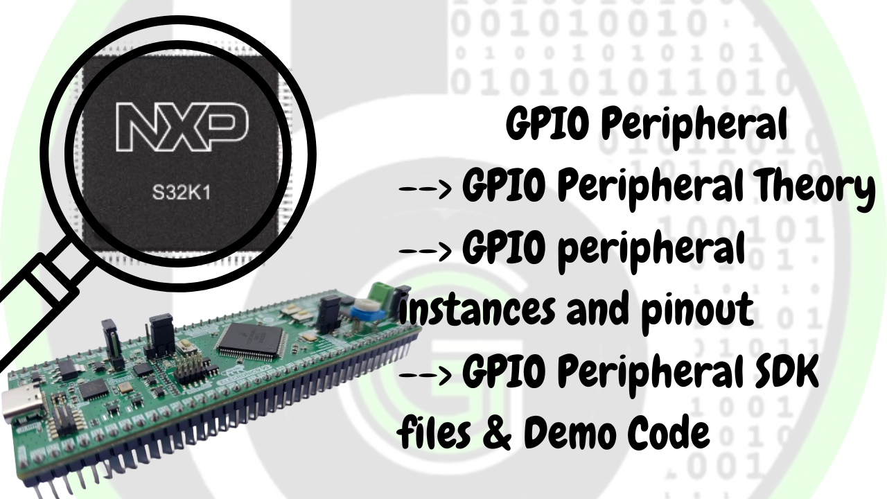
Table of Contents GPIO Theory So now we’ll talk about GPIO pins . GPIO stands for general purpose input output pins; they are the means for communication between the microcontroller and the external world (using sensors etc).It is signal that arrives on these pins or a signal that is sent or written on these pins that facilitates this communication. These pins can be configured to act as input or output via the application software(in our case stm32cube ide). The programmer can configure the pins as LOW or 0V or HIGH or 3.3V(or 5V ). These GPIO pins can also be configured to act as special purpose pins as well where their alternate functionality is exploited . These alternate functionality includes UART , ADC , SPI etc . In the case of UART communication, Transmitter(Tx) and Receiver(Rx) pins are required. GPIO pins can be configured to act as TX or RX pins . Even in ADC the pins are configured to act as Analog pins having 12 bits of resolution . The alternate functions of various pins are shown below: Input floating Input pull-up Input pull-down Analog Output open-drain Output push-pull Alternate function push-pull Alternate function open-drain GPIO Peripheral in STM32F103 All the pins of STM32F103 are grouped in multiple ports as PORT A, PORT B, PORT C As can be seen from Pin configuration chart in the PA1 stands for Port A Pin 1. There are 37 GPIO pins in stm32f103 which are divided as PORT A with 16 pins, PORT B with 16 pins, PORT C with 3 pins and PORT D with 2 pins. Each GPIO port has two 32-bit configuration registers (GPIOx_CRL, GPIOx_CRH), two 32-bit data registers (GPIOx_IDR, GPIOx_ODR), a 32-bit set/reset register (GPIOx_BSRR), a 16-bit reset register (GPIOx_BRR) and a 32-bit locking register (GPIOx_LCKR). In the register names, x stands for the port to which pin belongs. If we are configuring pin PA1, it has Port A then registers would be accessed by GPIOA_CRL and etc. Out of above-mentioned registers, GPIO peripheral has 2 most important registers: Direction Register(GPIOx_CRL, GPIOx_CRH)</h3 > Direction register: Set the corresponding pin as input/output pin. Data register(GPIOx_IDR, GPIOx_ODR)</h3 > Data register: where we set the Logic level (High (1)/Low (0)), for the corresponding pin if it is configured as output pin or we read the Logic level (High (1)/Low (0)), for the corresponding pin if it is configured as input pin. Pin Configuration Chart Pin Definitions GPIO Peripheral Block Diagram in STM32F103 First after selecting the pin the port is decided Then after following the arrow the busses are selected based on it: APB/APB1 or AHB After which the clock is enabled to the particular port using either __HAL_RCC_GPIOX_CLK_ENABLE() function or using the RCC AHB1 peripheral clock enable register and selecting the port to which clock has to be provided by enabling it. Methods to configure the GPIO Peripheral Configuring the busses i.e AHB1, AHB2, APB1, APB2 . The AHB bus is faster than APB bus and in case of certain modules they are connected to the same bus .Hence it depends upon the application which bus to use. As can be seen from the picture below the AHB1 takes clock to PORT A , PORT B , PORT C etc . Hence to initialize a pin to a particular port the in RCC AHB1 clock enable register GPIOEN is set to 1 (For Port A GPIOAEN , For Port B GPIOBEN etc) Enabling the clock to that port otherwise the particular pin will not be functional Creating an instance of the structure and then using the members of the structure set the following:- PIN – Takes the pin no as input GPIO_PIN_X {where X -0 to 15} MODE– Selects the mode the specified pin is supposed to work in . It takes in value Output Push Pull ,Output Open drain PULL- It selects the initial value of the pin and takes value no pull up no pull down, pull up or pull down SPEED- Selects the speed of the working of the specified pin i.e low, medium or high ALTERNATE- Specifies the alternate function performed by the pin UART TX OR RX , ADC etc, GPIO Peripheral SDK using STM32HAL We are going to use STM32 HAL SDK for using the GPIO peripheral of the STM32F103. STM32HAL is a very versatile and robust Software package for using Peripherals of the STM32 Microcontroller family. To know more about STM32HAL, refer to this link. Each STM32 HAL has drivers for all the peripherals of the STM32 Microcontroller(One can navigate to the Driver folder in the STM32F1 HAL local repo installed). These drivers can be configured and enabled to use in the project via the STM32 CubeMX configuration tool, which is also integrated into STM32CubeIDE( just like told in the above section for configuring GPIO peripherals). Will be digging into that part, in the next section. For now, let’s understand the STM32HAL GPIO SDK for STM32F103 MCU. stm32f1xx_hal_gpio.c: This file consists of various macros and is responsible for the intialization and configuration of the functions which in turn configures the peripheral. stm32f1xx_hal_gpio.h: consists of various structure definitions that help configure various parameters of the pin, enumeration, and various macros stm32f1xx_ll_gpio.c & stm32f1xx_ll_gpio.h: GPIO Low-level driver source/header file, contains functions that configure the GPIO Peripheral registers at the hardware level. These files are the ones that actually interact with the hardware and make it configurable to our needs.  STM32 HAL Functions for GPIO Peripheral Functions are set of instructions that required to perform certain tasks. In general, a function is first declared in header file(.h) and then it is definied in source file(.c) and then called in main.c or application code. It is of the form function return data type, function name and function arguments. In Embedded functions are required to initialize a peripheral or configure it on the basis of various parameters which are passed on using arguments. This information is then passed on to the registers. List of functions used
Clock Peripheral Theory Before getting into how to configure the clock peripheral . We will discuss why microcontrollers need a clock source at all. The processor , the busses and the peripherals that are present in the microcontroller all are reliant on the clock to synchronize their operations. The choice of the clock source depends upon the following factors:- How much speed is required for a particular application How accurate the clock source should be i.e the consistency of the period between each clock tick Power requirements of the application If there is any significant error in the clock speed it will cause unpredictable consequences for internal microcontroller operations.The operations such as:- The conversion rate of analog to digital signals is governed by a microcontroller clock . The clock determines the rate at which the analog signal will be sampled and how accurate that sampling is done is also governed by the accuracy of the clock. The digital to analog conversion in a microcontroller is also dependent on the clock as the clock speed determines the maximum frequency that can be generated for the analog signal. Also the clock accuracy determines the waveform accuracy In the case of asynchronous communication the sampling of the incoming data stream is clock dependent as well.Even though in some cases the synchronization of the clock is not necessary but the transmitter and receiver should have the same clock speed for decoding and encoding purposes. So in a nutshell the clock determines how fast a microprocessor executes the given set of instructions Clock Peipheral features in STM32F103 The main system clock of the microcontroller is the one from which all the other clocks are derived such as clock to AHB domain, clock to APB domain , clock to the USB, clock to the ethernet etc . This main system clock is referred to as the SYSCLK. As can be seen in the picture of the clock configuration setting the system clock after being chosen is passed through prescalers it gets divided into a clock source that goes into HCLK that goes into AHB bus , DMA , cortex system timer ,FCLK. PCLK1 that goes into APB1 peripherals and timer clocks .PCLK2 that goes into APB2 peripherals and timer clocks and ADC1. Hence it is responsible for operations such as DMA , ADC. These buses are further connected to the pins that are responsible for ADC , GPIO , SPI and other functionality and in case these pins are not being used the clocks to the pin can be disabled to save power FIG-1- Clock configuration in stm32cube To properly drive the SYSCLK there are 3 different sources:- HIGH SPEED INTERNAL (HSI) oscillator clock(Internal to MCU) HIGH SPEED EXTERNAL (HSE) oscillator clock(External to MCU) PHASE LOCKED LOOP(PLL) clock( Internal to MCU) There are secondary clock sources as well:- 40KHz low speed internal RC (LSI) this used to drive watchdog and optionally RTC(Internal to MCU) 32.768 KHz low speed external crystal (LSE) which drives the RTCclock (RTCCLK) the error involved the LSE is less compared to the LSI( External to MCU) By default the HSI is ON in the microcontroller whereas all the other clocks HSE, PLL etc are OFF. Each clock source can be switched ON or OFF independently when not in use to prevent unnecessary power consumption. HSI HSI is the default SYSCLK after startup from RESET state, wakeup from STOP OR STAND BY mode or failure of HSE. It is a low cost clock source having a start-up time less than HSE. The maximum frequency that can be generated is 8MHz using HSI. It suffers from the demerit that it is less accurate than external crystal oscillator or ceramic resonator Also as the temperature increases above 25 degree celsius the accuracy decreases HSE In case of high speed application HSE can be used as a clock source for SYSCLK . The HSE or the high speed external clock is an external clock that sometimes comes attached to the microcontroller itself or at times requires the usage of an external circuitry. HSE is faster and more accurate than HSI but suffers from demerits such as slower startup time, high power consumption and times usage of an external circuitry The maximum frequency that can be generated using HSE clock is 16MHz HSE has 3 states ON , OFF and BYPASS BYPASS is basically connecting wire to OSC_IN and putting the OSC_OUT in high impedance state i.e bypassing the crystal oscillator as can be seen in FIG-2 external source FIG-2 BYPASS mode in HSE PLL The PLL or phase locked loop is a clock system that is capable of providing the clock frequency much higher than that of HSI or HSE i.e in case of stm32f1 series it can go up to 72Mhz Hence for high speed applications PLL is a go to choice . Also peripherals such as USB, Ethernet PHY can not work using HSI or HSE. PLL provides the flexibility of choosing clock frequency without the help of an external oscillator. SYSTICK clock The SYSTICK is required to generate interrupts on a regular basis . It helps the OS in multitasking applications .In applications without an OS is used for timekeeping, time measurement or as an interrupt source. It is derived from the system clock in stm32 and has an usual value of 16MHz. Which means is to generate a delay of 1sec 16000000 has to be loaded on SysTick load value register Clock peripheral HDK in STM32F103 external oscillator pins MCO pins Clock peripheral SDK in STm32F103 Clock peipheral Files in STM32HAL: CLock peripheral low level files and HAL level files Fucntions descritption and structure decsritption Clock Peripheral HAL Functions HAL_RCC_OscConfig: return type HAL_RCC_OscConfig(RCC_OscInitTypeDef *RCC_OscInitStruct) Parameter arguments explanation and return type explanantion Argument 1 Argument 2 argument 3 return type //Demo of how to use functions Clock Peripheral HAL Data Types Data type name( structure name): //Code of that structure Tab #1 Tab #2 Tab #1 Lorem ipsum dolor sit amet, consectetur
What is PWM? PWM or Pulse Width Modulation, is a type of digital electrical signal which is periodic in nature, with a rectangular waveform. There are certain terms associated with PWM which we need to understand before we move ahead. Here’s a graphical representation of a PWM signal- · ‘Period’ = Tp , is the time it takes to repeat the same waveform · ‘Duty cycle’ is the time for which the signal is a logic 1 by the total time period. Ton is the time for which the pulse is high Hence, Duty cycle % = (Ton/ Tp) X 100 · ‘Frequency’ = F is the number of times the waveform repeats in a second. So, F = 1/Tp. Applications of PWM signals PWM signals have an extremely wide range of applications, here are a few of them- · Variable voltage generator– if you vary the duty cycle of a PWM signal and apply it to certain electrical components, the components act as if they are receiving analog signals. This is because the response time of the components is finite. So, components like LEDs, buzzers, brushed DC motors etc. can be controlled by PWM signals. Meaning, you could control speed of a motor, brightness of an LED or amplitude of a buzzer and so on. The voltage that they receive has a linear relationship with the duty cycle. So, if logic 1 is 5 Volts 0% duty cycle – 0V 25% duty cycle – 1.25 V 50% duty cycle – 2.5 V 75% duty cycle – 3.75V 100% duty cycle – 5V · As a control signal – Some electrical devices/components analyze PWM signals that they are receiving to give a corresponding output. So, changes in the duty cycle are reflected in the output. These include Servo motors, electronic speed controllers (ESCs) and many more. Here, the devices respond only to specific PWM duty cycles and frequencies If you take the example of servo motors, they can only be operated at 50Hz signal with a duty cycle of 2.5 % to 12% . Anything beyond that doesn’t result in the movement of the servo. (The frequency and duty cycles vary from among different servos, this is a very common value which most 180-degree servos respond to) Similarly, ESCs respond to a PWM signal with ON time of 1ms for minimum throttle and 2ms for maximum throttle with PWM frequency of 50 Hz. Some devices such as HCSR04 ultrasonic sensors give an output as a PWM signal in which the pulse width corresponds to the time it took for the ultrasonic wave to be received. How is PWM signal Generated on STM32?? Timer peripheral STM32 blue pill has 15 pins which can generate a PWM signal, with other models having even more pins for PWM generation. In this section, we will try to understand how PWM signals are generated by STM32 Every microcontroller has a built-in circuit which can measure the passing of time. These are called Timers. What timers essentially do is count up to a certain number and upon reaching that number, they change the value of a certain register to indicate that the timer has counted up to that number. Now, the time it takes to increment this count by 1 is determined by the timer’s clock frequency. So, if the frequency of a timer is 1KHz, its time period will be 1 Millisecond. Hence, if we count up to 10, we have measured the passing of 10 Milliseconds. This is how, by simply incrementing a number, timers can measure the time that has passed since the timer began counting. (This is how the HAL_Delay() function generates delays) The maximum count a timer can make is determined by its register size. So, an 8 bit timer can count up to 28 = 256, 10-bit timer –210 = 1024 16-bit timer –216 = 65536 32-bit timer –232 = 4294967296 So, a 1 bit increase in timer size equals to double the count Timers are extremely necessary for the functioning of a microcontroller as a lot of events in programs are time based, which you may not even realize. Timer Peripheral modes and features Coming to STM32 Blue pill, it has 4 timers of 16-bit size. To perform these functions, they need to be in specific modes. Here are all the modes in which timers can operate in STM32- 1. Input capture mode– In this mode, a pin on the board is set as input on which a PWM signal is sent by some device and we measure the frequency and duty cycle of that signal. This can be used to interface with devices such as HCSR04 ultrasonic sensors, which send a PWM signal as input to the microcontroller, where different parameters of PWM signals can be used to determine the distance which the sensor is trying to measure. 2. Output compare mode– In this mode, the timer is used as a counter and the count is compared to a register which contains a pre-programmed value, when they are equal, a software interrupt is generated and using this, a given pin is switched high or low. This mode comes in very handy when you are making a project which requires you to use multiple peripherals and at the same time generate a rectangular waveform of a given frequency and duty cycle, as it is interrupt based. 3. One pulse mode– In this mode, a pulse can be generated based upon a trigger from an input pin on the board , the pulse generation takes place after a certain delay from when the input trigger pulse was detected. This can be considered as a combination of mode 1&2 (IC &OC) 4. PWM generation mode– In this mode, we can generate a PWM signal on a given pin by fixing a frequency and a duty cycle. This is the mode we will be using to generate PWM signals through the main loop. The difference of this mode to mode 2 (Output compare
What is STM32 ? STM32 is a family of 32-bit Microcontrollers and development boards manufactured by ST Microelectronics which offer very high performance for a relatively low price. All STM32 microcontrollers are based on ARM Cortex-M processor which make them much better in terms of computing power than most of the common microcontrollers/microcontroller development boards which are available in the market. These microcontrollers also have been provided with software support by ST for developers for free. If you have experience with microcontrollers like Arduino, this is a great step forward in understanding microcontrollers in depth. The STM32 framework allows you to control all peripherals and allows you to tweak them as per your wish, whereas in Arduino IDE, when you program in C++, it comes with in-built functions and libraries which don’t allow you to understand the backend working behind everything. This is very crucial, as it allows you to use the microcontroller to its full potential. STM32 FAMILY The STM32 family of microcontrollers is vast and expansive, offering a variety of options for the consumer to choose from. The family of microcontrollers is broadly classified into 4 categories- High performance ST offers a series of microcontrollers which have the fastest code execution time, high speed data transfer and relatively higher flash memory. Along with this, the feature the most advance peripherals that ST offers. This makes these controllers very useful for real-time applications such as running an RTOS. STM32H7x The H7 series controllers are based on the ARM Cortex M7 offering very high speeds of upto 550Mhz. The microcontroller series comes in two variants, single core and dual core. Dual core H7 series controllers come with an ARM Cortex M4 core as well as an ARM Cortex M7 core which allows for processing work distribution, very useful for applications requiring many peripherals where response time is critical. The dual Core variants also come with an inbuilt SMPS as well. The single core series comes with an ARM Cortex M7 core with clock speed between 220-550Mhz, depending upon the variant. STM32F7x The F7 series controllers are based on the ARM Cortex M7, Thanks to an L1 (level 1) cache, the series delivers the maximum possible theoretical performance of the Cortex-M7 core. Cache memory temporarily stores instructions frequently accessed by the processor STM32F4x – The F4 series is based on the ARM Cortex M4. These controllers have less processing power then H7 and F7 series but still come with advanced peripherals and high flash memory. A very useful line of microcontrollers which offer a wide variety of features and come at a relatively lower cost than that of an F7/H7 controllers. The F4 series is broadly divided into 3 segments- 1.F4 Advance line- Offers up to 180Mhz of clock speed and a maximum of 2 Mb of dual bank flash memory, with advanced peripherals, consisting of communication buses such as QSPI. 2.F4 foundation line- Offer lower flash memory (between 512Kb-1Mb) , with few controllers offering advance peripherals and features such as camera interface and Ethernet MAC. 3.F4 Access line- This line of F4 controllers consists of entry level controller which can be termed ‘High Performance’. These controllers come with lower clock speeds, lower RAM but feature very good power efficiency, while also not compromising on peripherals. Wireless The main focus of the STM32Wx microcontroller family is wireless connectivity. They cover sub-GHz as well as 2.4Ghz frequency range operation The STM32 wireless MCUs are further divided into 2 categories– STM32WB These MCUs have a dual core processor unit, Cortex M4 & Cortex M0+, which allows for processing distribution, making it a great candidate for real-time processing and execution. The MCU series is based on STM32L4 architecture, which offers dynamic voltage scaling, reducing the power consumption of the device. They also support BLE 5.3, Open Thread and Zigbee protocols, making them a great choice for IOT applications, providing a lot of functionality onboard the chip itself. STM32WL These MCUs also come with a dual core processor unit like the STM32WB series, and some variants also come with a single ARM Cortex M4 as their processing unit. The key highlight of this series of microcontrollers is that not only do they work as a general purpose microcontroller, but also come with an integrated sub GHz radio supporting LoRa WAN which makes it a great choice for smart home applications, utilities, logistics, Industrial IOT etc. Ultra-Low Power – STM32 ultra-low-power microcontrollers offer designers of energy-efficient embedded systems and applications a balance between performance, power, security and cost effectiveness. The portfolio includes the STM8L (8-bit proprietary core), the STM32L4 (Arm® Cortex®-M4), the STM32L0 (Arm® Cortex®-M0+) and the STM32L1 (Arm® Cortex®-M3). The STM32L5 MCU (Arm® Cortex®-M33) with its enhancedsecurity features is the latest addition to this rich portfolio. The new STM32U5 series combines the latest and most efficient Arm Cortex-M33 core with an innovative 40 nm platform that reduces energy consumption to the bone, while increasing performance. The series also adds the state-of-the-art features which are required in today’s applications,including advanced cyber security with hardware-based protection, and graphics accelerators for rich graphical user interfaces. The STM32L5 series enhanced security features leverage Arm® Cortex®-M33 and its TrustZone® for Armv8-M. Thanks to this new core and a new ST ART Accelerator™ (also supporting external memory), the STM32L5 reaches an 443 CoreMark. The STM32L4 series offers the excellence of ST’s ultra-low power platform with an additional performance dimension by providing 100 DMIPS with DSP instructions and Floating-Point Unit (FPU), more memory (up to 1 Mbyte of Flash memory) and innovative features. The STM32L4+ series extends STM32L4 technology by offering higher performance (120 MHz/409 CoreMark executing from internal Flash memory), larger embedded memories (up to 2 Mbytes of Flash memory and 640 Kbytes of SRAM), and rendering advanced graphics without compromising ultra-low-power consumption. The STM32L0 series offers a genuine energy-saving solution for entry-level applications. Available in tiny packages down to 14 pins and with a wide range of Flash memory densities from 8 to 192 Kbytes, the STM32L0 features ultra-low power consumption in a competitive portfolio. Mainstream– The mainstream microcontrollers are more general-purpose boards
In the last post, we have gotten to know about the features of ADC Peripheral that we have in STM32 MCU. Now in this blog with the series of bare Metal Programming for Blue Pill, we will understand different register bytes and bits of ADC Peripheral to be used for using it in different features, configurations, and modes as we get to know about in the Previous Post. In this blog, we will be going through how to use ADC Peripheral for converting a Single Channel of ADC (only one ADC pin) and see its bare metal code. Single Channel Conversion Mode: Only one ADC pin is used, this mode is like when we have say connected only one analog sensor to one of the ADC pins of MCU like the Potentiometer is connected at PA0 pin. ADC Registers In depth for: Let\’s get into an in-depth understanding of which registers and their bits are used for configuring the ADC peripheral of Blue Pill in Single Channel Configuration. We will focus on bits and will give an explanation of why those bits are used for the 1. ADC_SR(ADC status Register) –>This register tells the status of ADC channel Conversion, as it name says. STM32F103 ADC Status Register: 11.12.1 Bit 1[EOC ]: This bit is set by hardware when a single channel of any group (Regular or Injected) is converted successfully. So this bit is used for monitoring when the ADC conversion is completed by using it inside the while loop if interrupts are disabled. 0: ADC Channel Conversion is not completed 1: ADC Channel Conversion is completed When hardware set this bit, we can clear this bit from the firmware end by setting the bit to 0 or by reading ADC_DR(ADC Data Register) Bit 4[STRT]: This bit is set by hardware when regular channel conversion has begun. So when we start the Regular Channel Conversion, we will use this bit inside the while loop to check that whether Regular Channel conversion has started or not. 0: No regular Channel Conversion has started 1: Regular Channel Conversion has started When hardware sets this bit, we can clear this bit from the firmware end by setting the bit to 0. Even if we don\’t clear this bit it will cause no effect during ADC Conversion. But its good practise to clear all bits of Status Register before starting the new conversion 2. ADC_DR(ADC Data Register) –> This register stores the converted digital data at a 12-bit resolution of the converted ADC channel. STM32F103 ADC Data Register 11.12.14 Bit 15:0 [DATA 15:0]: The ADC_DR is divided into two 16 bits groups. The first 16 bits from 0-15 contain the Converted value of the configured ADC Regular Channel. As our ADC is of 12-bit resolution, so this is left aligned or right aligned to 4 bits so as to get the 12 ADC converted data . Left Aligned or Right alignment of ADC Data Depends on ALIGN bit of ADC_CR2 So we will have following code and algorithm for ADC_SR & ADC_DR register:while(!(ADC1->SR & ADC_SR_STRT)) while(!(ADC1->SR & ADC_SR_EOC)); // wait till a group channel converstion has completed adc_data = ADC1->DR; //clear the EOC bit by reading DR register ADC1->SR &= ~ADC_SR_STRT; 3. ADC_CR1(ADC Configuration register 1) –> This register is used for the Configuration of ADC peripheral for Analog Watchdog Discontinuous Mode Interrupt Enable/disable Dual Mode configuration Scan Mode As we are not using any of these features, so all the bits for these registers will be set to zero, and to know about these features and their bit functions, u can navigate to corresponding blogs for those. STM32F103 ADC Configuration Register 1. 11.12.2 Bits 19:16 [DUALMODE 3:0]: These bits are used to configure the type of operating mode. In the blue pill, we have two ADC peripherals: ADC1 & ADC2. We can use these 2 ADC peripherals simultaneously by configuring the respective ADC in different modes or in independent modes. We are going to use these ADC in independent mode as will be using only ADC1 peripheral, so DUALMODE[3:0] will be set to 0. Bit 8[SCAN]: This bit is used to enable/disable the SCAN Mode feature in the ADC peripheral of BLUEPILL. Scan Mode is used when we convert more than 1 channel to scan all the configured channels in a Regular Group. As we are using only a single channel, means only one ADC pin is used so SCAN mode is not used and this bit will be set to 0. 0: Scan Mode disabled. 1:Scan Mode Enabled. So we will have following code and algorith for ADC_CR1 register:ADC1->CR1 &= ~(ADC_CR1_SCAN); // SCAN DISABLED, if using scan mode then dma must be enabled ADC1->CR1 &= ~(ADC_CR1_JDISCEN | ADC_CR1_DISCEN); // Discontinous mode disabled for both injected and regular groups ADC1->CR1 &= ~(ADC_CR1_DISCNUM_2 | ADC_CR1_DISCNUM_1 | ADC_CR1_DISCNUM_2 ); // no channels are configured in discontinous way. // if discontinous mode is enabled then number of //conversions to be done by discontinous mode has to be configured // DISNUM bits ADC1->CR1 &= ~(ADC_CR1_DUALMOD_0 | ADC_CR1_DUALMOD_1 | ADC_CR1_DUALMOD_2); // INDEPENDENT MODE SELECTED ADC1->CR1 &= ~(ADC_CR1_AWDEN | ADC_CR1_JAWDEN); // Analog watchdog disabled for both groups: regular and ibnjected 4. ADC_CR2(ADC Configuration Register 2) –> This register is used for the configuration of ADC Peripheral for: ADC Conversion enables/disabled for regular and injected groups and ADC peripheral enable/disable. Trigger source configuration for regular and injected groups. ADC Data Alignment, DMA, Continous, temperature sensor setting. STM32F103 ADC Configuration Register 2 11.12.3 Bit 0 [ADON]: ADC Peripheral On/OFF. This bit will be set to 1 to enable the ADC peripheral. All channel configurations and ADC Peripheral configurations have to be made before setting this bit to 1. 0: Disable ADC Peripheral 1: Enable ADC Peripheral Bit 1 [CONT]: This bit configures between Single Conversion mode and Continous Conversion mode. Continuous Conversion mode is selected when we have more than 1 ADC channel to be converted. As in this blog, we have
Home Category Child Category Introduction Imagine that we are building a robot or an interactive art piece. We might be interested in measuring temperature, distance to the nearest object, force, and acceleration, sound pressure level, brightness, or any other physical characteristics. The first step is to convert all these physical quantities into a voltage using a transducer. The world is analog in nature, so every quantity that we need to measure is measured by the transducer in an analog output. But our Computers, MCU, Processors are digital in nature, that is they can Understand only ‘1’ and ‘0’. Thus we need an interface that can convert analog values of the world into digital values so as to process them. Thus here comes the ADC(Analog to Digital converter) “Analog Signals need to be processed correctly before they can be converted into digital form. This processinbg of Analog Signal is done by Signal Conditioning circuits” Important Terms in ADC Resolution of ADC: As said, ADC transforms an analog voltage to a binary number(series of 1’s &0’s) which is then represented as a Digital Number over our screens. The Number of Binary digits (1 &0) that represents the Digital Number determines the ADC Resolution ADC Introduction in STM32 Like every modern family of MCU, STM32 too has inbuilt ADC. Now if we open the datasheet of STM32F103 Bluepill and Navigate to its ADC Section. Now let’s break down this ADC Introduction part to understand the ADC Peripheral in STM32 MCU Successive Approximation: Type of ADC which is used in STM32 MCU.Which is made using OPAMPS, Resistors, Digital & Analog Electronic Circuit. So depending upon the type of circuit their are different types of ADC. 1) Successive Approximation 2) Sigma Delta 3) Voltage to frequency 4)Dual Slope ADC Analog Sensors & Electronics are huge topic, so wont be able to cover everything & would be focusing on STM32 MCU ADC Peripheral Click Here12 Bit ADC : Resolution of the ADC Peripheral in STM32 MCUThis is Resolution of the ADC Peripheral in STM32 MCU.Means Decoded ADC value which we will get will be ranging from [0-4095] = 2^12Click Here18 Multiplexed Channels: Blue Pill we have 18 ADC pinsBasically channels means from which Analog Values of the External world/Transducer will be fed to the MCU. Out of the 18 Pins Blue Pill has 16 external and 2 internal sources. This means that in 1) 16 pins [ADC0-15], we can fed analog values from the external world, like interfacing some analog sensors 2) 2 pins[ADC16:17] have the internal analog sources (Internal temperature Sensor & Internal Reference Voltage) : There is one inbuilt Temperature sensor inside the MCU which Outputs the data in analog value & send it to ADC_Channel 16.Click Here Previous Next So that is for the basic introduction of the ADC peripheral of STM32F103, now let\’s dive into more in-depth to know about the features of ADC peripheral in STM32 MCU. ADC Features in STM32 MCU Regular and Injected groups In STM32 MCU ADC peripheral their is a feature of Regular and Injected Group, we can configure the ADC Channels to be either in Regular Group or Injected Group. Regular Group: ADC Channels which are configured in regular group are converted regularly( when ADC peripheral is started by setting ADC_CR2:ADON bit), just like basic ADC conversion of channels one by one Injected Group: Now Channels which are configured in injected group works on same principal of Regular Group but this group have higher priorty then Regular group. As it names says injected, this group will interrupt the Regular group Conversion Click Here Types of Conversion Modes in STM32 ADCTheir are 4 types of Channel Conversion Modes in STM32. 1) Single Conversion Mode 2) Continuous Conversion Mode 3) Scan Mode 4) Discontinuous ModeClick HereSingle Conversion Mode: As it name says \”Single Conversion\” so when ADC peripheral is configured to be in Single Conversion Mode , only one time conversion of configured ADC channels is done when ADC peripheral is triggered.Click HereContinous Conversion Mode:As it name says \”Continuous Conversion\”, so this is vice versa of single conversion. All the configured ADC channels are continuously converted once the ADC Peripheral is triggered by Software or by external event and converted data is continuously stored in ADC_DRClick HereScan Mode:This is 3rd type of Mode, as its name says\”Scan\”. So when configured in this mode, ADC works like a \”SCAN\”, it is used to scan a regular or injected group channel. In short, we can say if we are using more than 1 ADC channel & doing conversion of all configured ADC channels then we will be using Scan Mode. After the first channel conversion, it will go to the next configured channel for its conversion till the last channel configured Click HereDiscontinous Mode:This is 4th type of mode, in this mode we can convert configured channels of regular and injected group in short sequences of n conversion (n
first View What is a Processor Processor is programmable electronic circuitry that performs operations according to the instructions stored in memory. The processor as of itself does not have the memory and I/O devices. The processor reads the instructions stored in the memory, interprets it, and stores the output in memory or signals the I/Os. Processor Consists of the Processor core which contains circuitry for instruction fetching, decoding, and execution, register banks, and control units. According to the architecture design of the processor, the different processors have different components. For example, ARM cortex-M4 processors have NVIC, MPU, Floating point units, optional debug subsystems. This allows the microcontroller vendors to design differently. A block diagram of the microcontroller. Fig 1.2 – A microcontroller contains Many different blocks How does Processor control the world? Processors become an integral part of our life. We come across many devices which have processors embedded in them. For example: The smartphone on which I am writing this article has ARM cortex-A55 and cortex-A75 as processor, The Famous Tesla motors FSD Self-driving computer has many ARM processors. To give the idea of how processors are running the world look at these two examples. Upto 2019, Arm partners have shipped more than 160 billion Arm-based chips. Due to the shortage of semiconductor chips(processors) many car manufacturing companies had to reduce the number of cars manufactured. ARM Processor ARM Processor ARM processors are designed by ARM Ltd., ARM does not manufacture processors or sell the chips directly. Instead ARM licenses these designs to other semiconductor companies so that they can make their processor, microcontroller, SOCs as ARM processors are configurable. In the Cortex processor range, the processors are divided into three profiles: 1) The A Profile is designed to handle complex applications such as high-end embedded OSs. 2) The R profile processors are targeted primarily at the high end of the real-time market. These are applications, such as hard drive controllers, automotive systems, etc. 3) The M profile processors target smaller-scale applications such as microcontrollers and mixed-signal design. ARM CortexA1) The A Profile is designed to handle complex applications such as high-end embedded OSs.Click HereARM Cortex RThe R profile processors are targeted primarily at the high end of the real-time market. These are applications, such as hard drive controllers, automotive systems, etc.Click HereARM Cortex MThe M profile processors target smaller-scale applications such as microcontrollers and mixed-signal design.Click Here Previous Next ARM develops new processors, new instructions, and architectural features are added from time to time, as a result, there are different versions of the architecture. For example: ARM7TDMI is based on the architecture version ARMv4T. ARMv5TE architecture was introduced with the ARM9E processor families. With the ARM11 Processor family, the architecture was extended to ARMv6 with memory system features and SIMD instructions included. Cortex family processors are based on ARMv7 and ARMv6. The cortex-M3 and cortex-M4 processors are based on ARMv7-M architecture. The architecture evolution of the ARM can be seen in the following (Fig 1.4). All the cortex-M processors support Thumb-2 technology(16-bit and 32-bit instructions), with no need to switch the processor between Thumb state and ARM state. Keil MDK-ARMIAR systems(Embedded workbench for ARM Cortex-M) GCC_based IDEs Previous Next For Programming and debugging ARM Processor based MCU’s, we will be using Microcontrollers of different vendors like: STMicroelectronics and NXP Semiconductors. We will be using STM32 Family of STMicroelectronics and S32 Family of NXP Semiconductors. Both of these are based on ARM Processor and have rich set of features and specifications which are ideal for learning embedded systems. Now both the companies provide their own IDE’s for : STM32CubeIDE and S32 Design IDE for respective family of MCU mentioned above. Or we can also use the Above-mentioned IDE’s which are general IDE’s can be used to program any ARM processor based MCU. But recomended one is to use Vendor specific IDE as it has many extra featutes for programming. CMSIS The Common Microcontroller Software Interface Standard(CMSIS) was developed by ARM to allow microcontroller and software vendors to use a consistent software infrastructure to develop software solutions for cortex microcontrollers. THE AIM OF CMSIS: Software reusability: make it easier to reuse code with different Cortex-M processors, reducing time to market and verification efforts. Software compatibility: Due to consistent software infrastructure, software from various sources can work together, reducing the risk in integration. The CMSIS allows easy access to processor core features from the c language. CMSIS-compliant device drivers can be used with various compilation tools. CMSIS started out as a way to establish consistency in device-driver for the Cortex-M microcontrollers, and this has become CMSIS-Core. Since then, additional CMSIS projects have started: CMSIS-Core A set of APIs for applications developers to access the features on the Cortex-M processor regardless of microcontroller devices and toolchain used. CMSIS-DSP library This library is intended to allow software developers to create DSP applications on Cortex-M microcontrollers easily. CMSIS-SVD the System View Description in an XMl-based file format to describe peripheral set in microcontroller products. CMSIS-RTOS the CMSIS-RTOS is an API specification for embedded OS running on Cortex-M Microcontrollers. CMSIS-DAP the CMSIS-DAP(Debug Access Port) is a reference design for a debug interface adaptor, which supports USB to JTAG/Serial protocol conversions. The CMSIS files are integrated into device-driver library packages from the microcontroller vendor. So when you are using CMSIS-compliant device-driver libraries provided by the microcontroller vendors, you are already using CMSIS. We can define the CMSIS into multiple layers: Core peripheral Peripheral Layer Name definitions,address definitions, and helper functions to access core registers and core peripherals. This is processor specific and is provided by ARM. Device Peripheral Access LAyer: Name definitions, address definitions of peripheral registers etc. This is device specific. Access Functions For Peripherals Access Functions For Peripherals How do I use CMSIS-Core ? Add Source files to the project. This includes: Device specific, toolchain-specific startup code, in the form of assembly or C. Device-specific device initialization code(e.g. System_c). Add header files into the search path of the project: A device-specific header
- 1
- 2