SPI Peripheral in S32K144
Explore this blog to know about SPI peripheral in NXP S32K144 MCU

Explore this blog to know about SPI peripheral in NXP S32K144 MCU
Explore this blog to know about UART peripheral in NXP S32K144 MCU’s

Explore About PORT Peripheral in S32K144 MCU || What is it? How to use it? How is it different from GPIO Peripheral
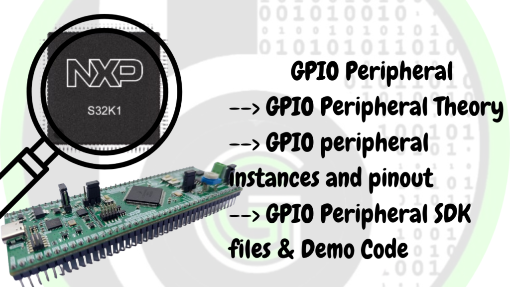
Explore About GPIO Peripheral in NXP S32K144 MCU || What is it?? How to use it??
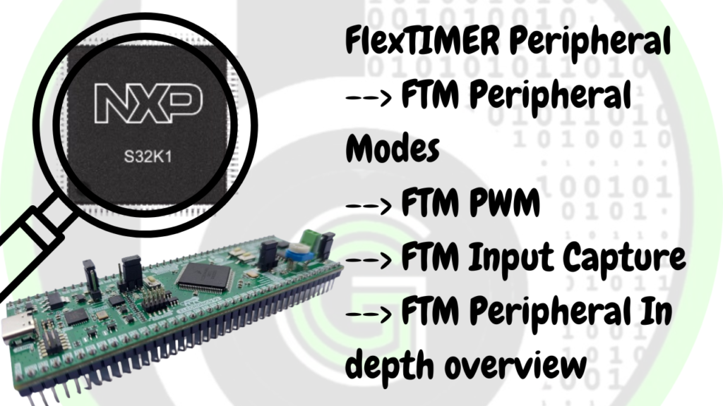
Explore about FTM Peripheral of Automotive MCU S32K1xx using ElecronicsV3 Board (S32K144 MCU) || FTM PWM || FTM ICU || FTM Counter Modes

Explore about ADC Peripheral of Automotive MCU S32K1xx using ElecronicsV3 Board (S32K144 MCU) || ADC Channels || ADC HW&SW Triggering || ADC Pre Triggers || ADC relation with PDB and TRGMUX

Learn how to use FlexTIMER peripheral of Automotive MCU S32K1xx using ElecronicsV3 Board (S32K144 MCU) by understanding FlexTIMER peripheral.
Interfacing10KOhm Potentiometer using ADC Driver of Autosar MCAL Layer via ElecronicsV3 Board (S32K144 MCU)
Prerequisites for PDB of ADC What is the PDB? The PDB is a powerful peripheral in microcontroller’s designed to provide
About FlexTimer Module: Timer peripheral in NXP S32K1xx and S32K3xx Automotive Microcontrollers