Overview

So hello guys, welcome back to another series of Microcontroller tutorials. As Microcontrollers are new big thing happening across the globe, but to learn about microcontrollers becomes quite challenging as most of the content on web is theoretical based and quite unorganized. Or the content is only roaming around 2-3 microcontrollers (Arduino, ESP or PIC), even though there are number of Microcontrollers of different vendors. Also, framework of Arduino and Arduino IDE hides most of the things that are going inside the microcontrollers.

Here at Gettobyte, you will get content on microcontroller tutorials for different vendors and much more via practical way. Which will help you to learn important skills to build you Carrer on Semiconductor Industry and also help you in product development/DIY projects for different Industries, so as to make embedded devices with Industry standard Microcontroller.

Would recommend viewers to read below blogs, if you are newbie, who is just coming from Arduino environment and wanna explore microcontrollers and wanna build Carrer into semiconductor industry, then this blog will give you overview of what all things are there to be needed for making projects and to play along with the different microcontrollers.

Table of Contents

This Time we are going to start with NXP Semiconductors S32K144 automotive MCU. Objective of this blog, will be to:

  • –> Learn About NXP Semiconductors.
  • –> Get to know about S32, S32K & S32K144 Platform of NXP Semiconductor.
  • –> Hardware Development Kit of S32K144 MCU.
  • –> Software Development Kit of S32K144

After this Introduction blog on s32K144 MCU, we will be doing hands on different peripherals of this MCU starting with GPIO, UART, I2C, SPI and…

About NXP Semiconductor

NXP Semiconductors is a global semiconductor company that designs and produces a broad range of semiconductor solutions providing hardware and software for them. It is a fabless company that designs the Microcontrollers, Microprocessor, ASICS’s and other discrete electronic components, targeting the industries like but not only limited to automotive, industrial automation, communication infrastructure, IoT, Robotics, Medical, Consumer Electronics, drones and Security Chips.

Apart from these chips and IC’s, NXP semiconductors also provide software to run these chips and demonstrating different applications where its products can be used. NXP semiconductor also works in AI/ML and edge computing.Making it not only giant hardware-based semiconductor company but software company too.

History of NXP Semiconductors roots back to 1950’s. It was founded in 1953 as part of the electronics giant Philips, at that time the company name is Philips Semiconductors. In 2006 it become independent company and its name changed to present name: NXP Semiconductors. After that it had acquired several companies and had done partnership deals with companies like Silicon labs, STMicroelectronics, Trident Microsystems, Conexant Systems and to expand its product lines and business revenue. In March 2015, merger agreement was announced through which NXP semiconductors acquired The Freescale semiconductors. After this merger NXP semiconductor become one of the largest semiconductor companies in the world. Both NXP and Freescale had deep roots stretching back to when they were part of Philips (NXP), and Motorola (Freescale). NXP primarily focusing on near field communication (NFC) and high-performance mixed signal (HPMS) hardware, and Freescale focusing on its microprocessor and microcontroller businesses. NXP semiconductor chips are used in almost every electronic gadget we see around us. To know more about NXP semiconductors, one can navigate to NXP website and Wiki page.

In this blog we are going to start with Automotive Industry. NXP semiconductors has a S32 Platform of microcontrollers and microprocessors specially targeting the Automotive industry. S32 platform has all the kind of MCU’s and MPU’s targeting different Domains of Automotive. There are broadly five domains in automotive:  Power Train, Chassis, Body & Comfort, HMI, and
Telematics. These 5 domains cover all the devices embedded in Automotive.

About NXP S32 Platform

S32 is a series of Microcontroller which are designed and manufactures by NXP Semiconductors, specially targeting for automotive applications but not only limited to them. Then with in S32, there are further categories as S32K, S32G, S32R, S32V.

NXP S32 Product Platform

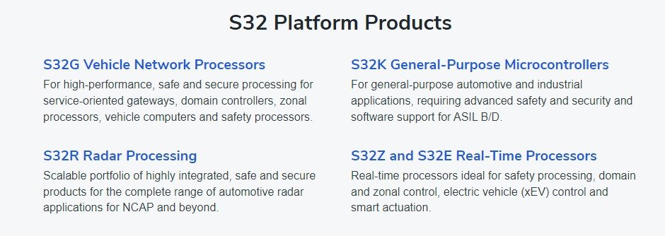
Each of the category, can be used in one of the domains of automotive. Like say in powertrain one can use S32K for motor control applications and for telematics one can use S32R for radar processing, to get information about nearby objects. This is what something ADAS system is. Like when some car come nearby to a car, some sensor senses that distance (That is telematics zone) and after a certain threshold car speed automatically changes by controlling its motor RPM (that is part of powertrain).

NXP S32 Platform is being designed, providing end to end solutions for Automotive Industry. Not only MCU’s and MPU’s but NXP also provides large number of tools and software to build the applications for Automotive from S32 Platform. Dedicated IDE, Debugging tools and drivers, Real-time Drivers (RTD), RTOSes(FreeRTOS, Zephyr, NXP RTOS) and Autosar complaint SDK.

Almost every MCU of S32 family has support of Automotive protocols: CAN, LIN, FlexIO and etc. Ranging from ARM CortexM3(single core) to ARM Cortex A9(triple core). Having advance features to support automotive needs like : Hardware security modules(HSM) for safety and security, High Bandwidth Ethernet and USB support for connectivity and etc.

We are going to start with S32K312 MCU, which is part of S32K family. It is based on ARM Cortex M7 and has dedicated HSM-H that too upto EVITA specs and also ASIB/D complaint. Making it a perfect MCU to start for building general purpose Automotive applications.

Would get to know more about S32 platform along with tutorial series on S32K312 MCU. 

S32K MCU family series

We are going to start with S32K platform which are general purpose Microcontrollers designed to make different ECU in zonal and body control modules for automotive applications.

NXP S32K1 MCU series

S32K is further categorized into S32K1 and S32K3 series. S32K144 is part of S32K1 series.

About S32K144 MCU

S32K144 MCU is part of the S32K series of MCU of NXP, which are General purpose Microcontrollers for developing body & control, powertrain related applications automotive Industry. S32K144 is single core ARM cortex M4F processor based MCU with rich set of peripherals for Automotive Industry.

  • It has upto 89 General Purpose Input/Output (GPIO) pins for connecting large number of I/O sensors and modules to act as HMI, thus perfect choice for acting as ECU node in domain or zonal Architecture of E/E automotive.
  • It has 512 KB of on chip flash memory and 256KB of SRAM with ECC feature to have secure memory regions.
  • It operates at Voltage range (Vdd) of 2.7V to 5.5V, with temperature range of -40 to 150 degree Celsius.

Means if Voltage of 2.7V is supplied to IC then it will recognize input signal of 1.89V(0.7* Vdd) to 3V (Vdd+ 0.3) as High signal and input signal of -0.3V(Vss-0.3) to 0.81V(0.3*Vdd) as Low Signal. If Voltage of 5.5V(Vdd) is supplied to IC, then it will recognize input signal of 3.5V(0.65*Vdd) to 5.8V(Vdd+0.3) as High Signal and input signal of -0.3V(Vss-0.3) to 1.9V(0.35*Vdd) as Low Signal.            (Analyzed from DC electrical specification of S32K1-DS)

Thus, IC can be used to measure Input signals for low voltage sensors like accelerometers, Capacitive and Inductive sensors.

  • S32K144 IC has Arm Cortex M4 core, with Integrated DSP, Configured NVIC, Single Precision FPU and Debug CoreSite architecture. ARM Cortex M4 Core supports ARMv7 Architecture and Thumb2-ISA.
  •  IC can run up to at 112MHZ frequency when running at System Phase Locked Loop (SPLL). It has Fast Internal RC Oscillator (FIRC), Slow Internal RC Oscillator (SIRC), Low Power Oscillator (LPO), Real Time Counter External clock (RTC_CLK).
  • ADC peripheral is essential for applications involving Electrification. Thus, IC has two 12-bit SAR ADC modules of 16 channels. IC also has 8-bit internal DAC module for integrating power IC\’s in the case of electrification.
  •  IC also has onchip Debug facilities of Serial Wire Debug (SWD), Serial Wire Output (SWO) and JTAG combined. And IC inherits the CoreSight Debug Architecture of ARM processors.
  • In terms of On-board Communication peripherals. IC has 3 Low Power SPI, Low Power UART and FlexCAN peripheral, 1 Low Power I2C, one FlexIO module for emulation of on board communication protocols. Various and Different types of Automotive Sensors and modules can be connected along with this IC with rich support of Communication peripherals.
  • Automotive involves high secure and safety ECU nodes. Thus, IC has Cryptographic Service Engine (CSEc) implemented. It includes AES-128,CBC,ECB and CMAC. Pseudo and True Random Number Generators(PRNG,TRNG) with sequential, parallel and strict Boot Mode.
  • In addition TO CSEc, IC has Error Correction Code(ECC) and Cyclic Redundancy Check module, system memory protection units with Internal(WDOG) and external(EWM) Watchdog monitor.
  • For offloading the load on CPU while transferring data from memory regions of chip, IC has 16 channel DMA with 63 requests sources using DMAMUX.
  • IC also has Timing and Control module for capturing and outputting digital signals. It has 4 16 bit FlexTimers Module(FTM), 1 16 bit Low Power Timer Module(LPTMR),  1 32 bit Low Power Interrupt Timer(LPIT) and 1 32 bit Real time Clock(RTC).
  • IC comes only in LQFP packaging of 48,64 and 100 pins.

S32K144 MCU Block Diagram


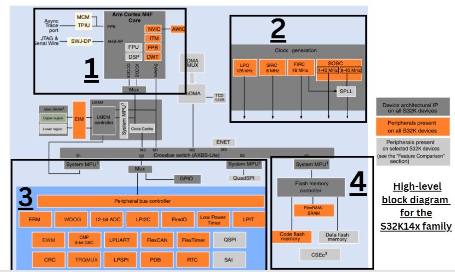
Above is the high-level architectural view of S32K144 MCU. As told in my previous blogs, one can consider Microcontrollers as human body, in which there is one human brain and all other body parts are connected to it, to interact with outside world. In the case of Microcontrollers brain is processor and peripherals connected to processor are body parts. 

  • The first block in above diagram is ARM cortex M4F Processor, which is most important unit of MCU. It has additional features integrated in it like that of NVIC,DSP, Debug and etc. as one can see in the block diagram.
  • Second block is clock generation. As digital systems need to run at some frequency that is provided by clock peripheral. So this block takes care of generating clocks for various sub-units of MCU by having different clocks as shown in block diagram.
  • Third block is the analogous to body parts of human body that interact with outside world. Here 3rd part comprises of wide number of on chip peripherals, which are connected to external sensors or modules to have interaction with external world.
  • Fourth block is the memory block, which comprises of flash memory, SRAM and memory protection features.
  • These are the main 4 blocks which covers majority of IC features, but in addition to it there are also small blocks like DMA, CSEc and etc. which would be further discussed in upcoming blogs.

S32K144 Hardware Development Kit(HDK)

ElecronicsV Series: Arduino of Automotive World

ElecronicsV is a Automotive Development Board Series, supporting various automotive technologies like: Autosar MCAL layer, Matlab Model Base Designing, Vehicle communication protocols like” CAN, LIN, JN5189, Hardware Security Module based on SHE standard for providing safety/security support and advance motor control application for mobility applications.

These Development boards are built on automotive microcontroller S32K144 which are based on ARM Cortex M4 Processor and has various on-board features to enable the hassle-free development and learning of automotive technologies.

There are in total 3 versions in ElecronicsV series:

  1. ElecronicsV1: Breadboard Compatible Development board based on S32K144 MCU with basic on-board features of RGB LED’s, Switches,  Potentiometer and UART. This Board is obsoleted now. It was launched in July 2023.
  2. ElecronicsV2: Breadboard Compatible Development board based on S32K144 MCU with on-board features of RGB LEDs, Switches, Potentiometer, UART over Type C Cable and CAN transceiver IC making ElecronicsV2 self-sufficient CAN Node. This Board is also obsoleted now. It was launched in September 2023.
  3. ElecronicsV3: Breadboard Compatible Development Board based on S32K144 MCU with on-board features of: RGB LEDs, Switches, Potentiometer, BNO055 IMU Sensor, On-Board Jlink Debugger via Type C cable, CAN FD transceiver IC making ElecronicsV3 self-sufficient CAN Node and Virtual UART COM Port. This board is latest product and available in stock. It was launched in June 2024.

For buying the ElecronicsV3 board: S32K144 Elecronics V3 with onboard J-Link, BNO055 and CAN – Electronics Infra

ElecronicsV3 board is great amount of value of money at 6,000 INR. At just 6,000 INR, one can learn and get exposure to automotive technologies which are highly valued in the industry and great in demand. As usually other automotive hardware kits supporting all these technologies comes at heavy and heft prices of about more then 15-20K. Also, For ElecronicsV3, a full getting started and in-depth resources are they’re at: ElecronicsV(S32K144 MCU) – Get To Byte

Elecronicsv3 Board Pin Out

 
PINOUT of NXP S32K144 Evaluation Board

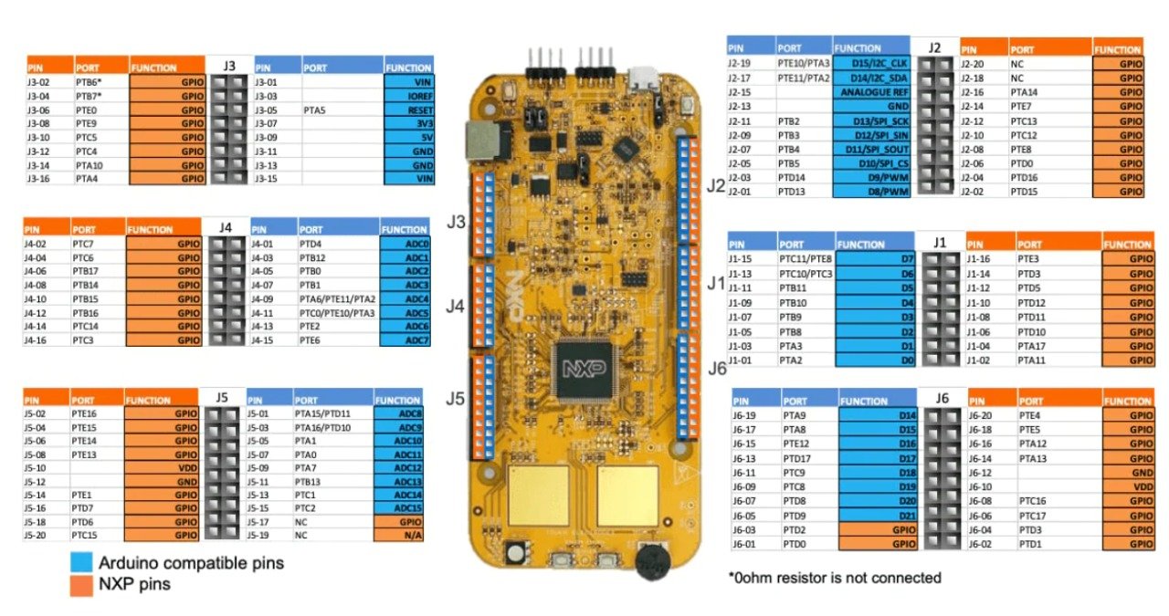
Above is the pinout of Evaluation board. We can easily connect sensor and modules via Jumper wires. Also the board has Arduino uno compatible expansion shield support.

  1. The board has on-board Mini High speed CAN Transceiver and System Basis Chip: UJA1169TK.( CAN_TX –> PTE5&CAN_RX –> PTE4).
  2. Single and multichannel LIN transceivers: TJA1027( LIN_TX–> PTD7 & LIN_RX -> PTD6).
  3. 2x touchpads(PTC3&PTC0), 1x Potientiometer(PTC14), 1x RGB LEDS( RED: PTD15, Blue: PTD0 and Green: PTD16) and 2x push buttons.

Debuggers

For Programming ElecronicsV series of Board, one can debug via Segger Jlink Debuggers or Even PEMicro Debugger via SWD protocol which is accessed via on-board 10 pin Debug connector pins.

ElecronicsV1 and ElecronicsV2 doesn’t have on-board Jlink Debuggers, for those board we will be needing external Jlink Debuggers for programming and debugging the S32K144 Microcontroller. Those who are interested in getting Jlink Debuggers for NXP S32 Family of MCU, can have a look at our ProBug Debugger. Which is Jlink debugger indigenously developed by Gettobyte.

ElecronicsV3 has onboard Jlink debugger and that too with virtual UART COM part, which makes it very easy and cost-effective enablement on automotive technologies. User just need to connect USB Type C cable from the ElecronicsV3 board to Host PC/Desktop. And now you are good to go. Doesn’t need anything else.

S32K144 Software Development Kit

IDE(Integrated Development Environment)

NXP provides the Integrated Development Environment especially for S32 platform products, S32 Design Studio which is built on Eclipse IDE.  S32 Design studio is based on open-source GNU Compiler collection (GCC) and also has GNU debugger (GDB).

S32 Design Studio Home page

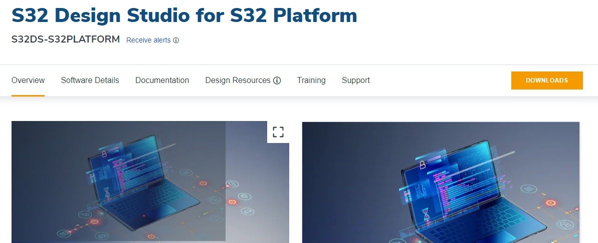
One can easily download the S32 design studio from NXP website after logging in from here.

S32 Design Studio also provides various features for debugging and flashing the firmware. In addition to that we can add various extensions and install SDK packages of S32 platform directly from S32 design Studio.

S32 Design Studio is the Integrated Development Environment (IDE) which is used for writing, building and debugging the code to run on S32K144 MCU. S32 DS has many inbuilt features for debugging and analyzing the code, for efficient and fast implementation. Steps to install S32 Design studio are pretty straight forward and can be referred from here. Am skipping that part as that is pretty well documented on NXP Website and directly moving to GPIO Peripheral specific API’s and Files.

SDK(Software Development Packages)

NXP also provides built-in Software packages for fast development of applications: S32 Software Development Kit for S32K1. The SDK includes: Real Time Drivers, FreeRTOS support, Ethernet Stack, NXP motor control Libraries and etc. The SDK support 5 compilers for compilation: GCC, GreenHills(GHS), ARM Compiler, IAR and WindRiver DIAB.

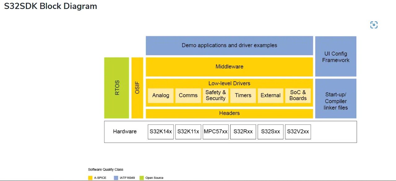
Now there are 2 SDK’s, which are provided for S32K144 MCU by NXP Semiconductors.

One is Autosar 4.4.0 complaint, in which all the peripheral drivers and RTD’s of the MCU peripherals are build based on Autosar classic standard. For the sake of refernce thorughout the series i will be naming this SDK as Autosar Complaint Drivers for S32K. Naming convention of these are like this: SW32K1_RTD_4_4_1_0_0_D2108

And other is generic one, based on MISRA C guidelines and Standards in which all the peripheral drivers, RTD’s and other software stacks (FreeRTOS and middleware: TCP/IP) are built on easy-to-use architecture, with less abstraction layers and complexities as compared to Autosar based for easy to use. Would be naming this as S32K Software Development Kit (S32 SDK). It boast an impressive array of features, including a comprehensive suite of robust hardware abstraction layers, peripheral drivers, RTOS, stacks, and middleware. These tools are specifically designed to simplify and accelerate the application development process, making it easier for developers to create high-quality applications with ease. Naming convention for these are like: S32_SDK_S32K1xx_RTM_4.02


S32K SDK

We will be using SDK based on MISRA C guidelines and standards, the S32K Software Development Kit at first: S32SDK_S32K1xx_RTM_4.0.2.

S32K Software Development Kit (S32 SDK) boasts an impressive array of features, including a comprehensive suite of robust hardware abstraction layers (HAL), peripheral drivers, RTOS, stacks, and middleware. These tools are specifically designed to simplify and accelerate the application development process, making it easier for developers to create high-quality applications with ease

As This SDK can also be downloaded easily from website. Am skipping the part of its installation part, in case of any Douts do reach out to me.

S32K Software Development Kit consists of several key components that can be used for Application development. When we download the package of S32K SDK, one will see following folder structure:

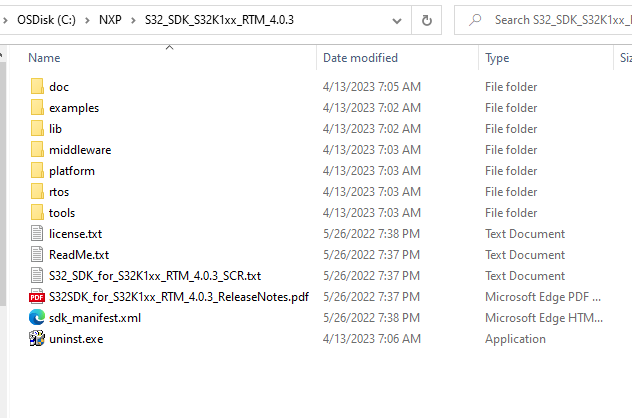
//just some overview on what each folder does!

We will be initially focusing on Hardware Abstraction Layer and peripheral drivers. For that folder platform is key component. Under the Platform, their are 3 folders as shown below:

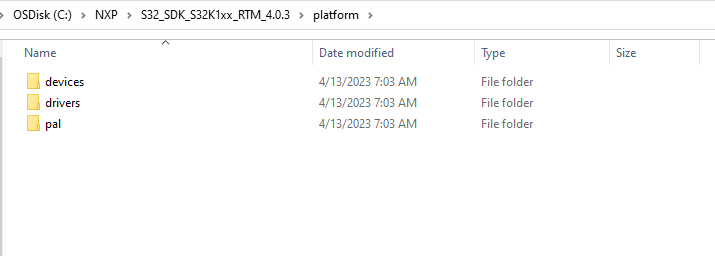
  • devices folder: contains the controller specific register header files, core specific register header files, controller specific feature configuration file, linker scripts and startup codes for different S32K MCU’s.
  • drivers folder: this contains the low level drivers for the peripherals of the MCU. Depending on the configurations done, low level drivers would be implemented.
  • pal folder: this contains the Peripheral Abstraction Layer for providing the unified interface for families of peripheral, allowing for cross -platform compatibility of application code.

As we are using S32K144 MCU, so we will find 2 files in devices folder: S32K144.h & S32K144_features.h files.

These are kind of configuration files, peripheral register address files and enables/disables the features that are to be supported in S32K144 MCU. These 2 files are one of the key files and would be used time to time.

				
					/*
** ###################################################################
**     Processor:           S32K144
**     Reference manual:    S32K1XX RM Rev.13
**     Version:             rev. 4.4, 2021-04-26
**     Build:               b210426
**
**     Abstract:
**         Peripheral Access Layer for S32K144
**
**     Copyright 1997-2016 Freescale Semiconductor, Inc.
**     Copyright 2016-2021 NXP
**
**     NXP Confidential. This software is owned or controlled by NXP and may only be
**     used strictly in accordance with the applicable license terms. By expressly
**     accepting such terms or by downloading, installing, activating and/or otherwise
**     using the software, you are agreeing that you have read, and that you agree to
**     comply with and are bound by, such license terms. If you do not agree to be
**     bound by the applicable license terms, then you may not retain, install,
**     activate or otherwise use the software. The production use license in
**     Section 2.3 is expressly granted for this software.
**
**     http:                 www.nxp.com
**     mail:                 support@nxp.com
**
** ###################################################################
*/
/*!
 * @file S32K144.h
 * @version 4.4
 * @date 2021-04-26
 * @brief Peripheral Access Layer for S32K144
 *
 * This file contains register definitions and macros for easy access to their
 * bit fields.
 *
 * This file assumes LITTLE endian system.
 */


					/*
 * Copyright (c) 2015 Freescale Semiconductor, Inc.
 * Copyright 2016-2020 NXP
 * All rights reserved.
 *
 * NXP Confidential. This software is owned or controlled by NXP and may only be
 * used strictly in accordance with the applicable license terms. By expressly
 * accepting such terms or by downloading, installing, activating and/or otherwise
 * using the software, you are agreeing that you have read, and that you agree to
 * comply with and are bound by, such license terms. If you do not agree to be
 * bound by the applicable license terms, then you may not retain, install,
 * activate or otherwise use the software. The production use license in
 * Section 2.3 is expressly granted for this software.
 */

/*!
 * @file S32K144_features.h
 * @brief Chip specific module features
 *
 * @page misra_violations MISRA-C:2012 violations
 *
 */


Run Time Debugging Tool: FreeMaster

FreeMaster Run-Time debugging tool

 FreeMaster Run-Time debugging tool

NXP Also provides the FreeMaster tool for run-time debugging. We will get onto this in upcoming blog, for the time being we are going to start with S32 Design Studio and S32K1 SDK.

Getting Started

 Getting Started with S32K144 Evaluation Board

We will get started with NXP S32K144 EVB board by running the Hello world program. In Microcontroller world Hello World example is Blink LED project. But before that we need above mentioned IDE and SDK for setting up the environment of S32K144 to do cross compilation in our Desktop/Laptop.

Refer this link: Get Started with the S32K144EVB | NXP Semiconductors for IDE, SDK installation and building Hello World program on S32K144 Evaluation board. Starting from the next blog we are going to develop application projects by interfacing different sensors and modules.

Further blogs to read
ARM Coresight: Debug and Trace in Embedded System

Table of Contents Definition of ARM CoreSight \”CoreSight is the Debug Architecture from ARM for Debugging and Trace Solutions in Complex SoC designs (Single core and Multi core)\” CoreSight Provides all the Infrastructure that is required to Debug, Trace, Monitor, and optimize the performance of a Complete System on Chip (SoC)Design. The Debug and Trace Features of the ARM Cortex M processors (M3/M4/M33/M7/M0, etc.) are designed based on the CoreSight Debug Architecture. This Architecture Covers a Wide Area Including Debug Interface protocols, on chip bus for debug access, Control of debug components, security features, trace data interface and more. Debug and Trace in Embedded Systems By now one obvious question to beginners or newbies that must have come in their mind is what is Debug and Trace. What are these features for which we have a whole complete Architecture called CoreSight? Why do we need Debug and Trace solutions in our Processors/Embedded Controllers? Is it not? For those readers They can check out this blog, providing you clarity and understanding of all such questions. One can Understand Debug and Trace Feature/Functionality as one of the Block/Unit of the Processor. Just like We have UART, SPI, I2C, etc. peripherals for our Microcontrollers for which we have separate Block, Architecture, Peripheral Memory Registers for accessing them and Communication Protocol pins in our Microcontroller. Same Way-out Debug/Trace is one of the peripherals which is present in our Processor for which it has its whole architecture and above Marked things. ARM Processor has CoreSight Architecture. MIPS Processor has EJTAG Architecture. IBM PowerPC processor has COP. (Units/Block of the Processor are not called peripherals, I have used the above term just to make u understand the analogy) What are Debug Features?? Features are used to observe or modify the state of parts of the design. This is also Called Invasive Debugging Execute instructions line by line function i.e., halting the processor after execution of each line of code(single stepping). Execute Instructions Function by function i.e., halting the processor after execution of each functions (Step Over) Return from the Function (Step Return/Step Out) Stop the processor (halting) Stop the Processor at a particular à line of code (called Breakpoint) àmemory address (Called Watchpoint) à coded condition of a variable or memory address is achieved (Conditional Breakpoint/Watchpoint) On can control the program execution (By points 1-5)so as to examine(Both read or Write) the change in value of bits of the MCU Peripheral registers and Core Processor Registers (like examining the contents of UART peripheral Registers to mark at which line of code data is received or transmitted by seeing the UART Status registers which has corresponding bits to indicate the event of receiving and transmit data). Debug frequently involves halting execution once a failure has been observed and collecting state information retrospectively to investigate the problem. There are 2 Communication Protocols For using Debug Features: SWD & JTAG JTAG is an industry Standard protocol (IEEE 1149.1) which is used for debugging and boundary scan testing. It is the de facto Serial Protocol which is present in almost every Processor Family other than ARM also like AVR 8 core, MIPS, PowerPC, etc. To be noted down: JTAG Requires 4 pins: TCK, TDI, TMS, TDO; the recent signal TRST is optional. ARM CoreSight Technology introduced the 2 wire Protocol SWD (Serial Wire Debug): SWCK and SWDIO which is used for Debugging all the ARM based Processors. The Serial Wire debug(SWD) protocol provides the same debug access features and supports parity error detection, which enables better reliability in systems with higher electrical noise. Therefore, the Serial Wire debug protocol is more favorable then JTAG Interface. Also, SWD and JTAG debug protocols share the same Connections: TCK and SWCL use the same pin, TMS and STDIO use the same pin.  The SWD port alone does not allow real-time tracing. What are Trace Features?? Trace refers to the process of capturing data that shows information about how the components in a design of a firmware are operating, executing, and performing. This is also Called Non-invasive Debugging. It is real-time (with a small timing delay) and can provide a lot of useful information without stopping the processor. Information like: Amount of execution time for each function(Statistical Profiling) Call hierarchy and execution time sequence of functions Event Execution timing(Timestamp) Clock cycles taken for execution of a particular Instruction. Examine or change the contents of the memory or peripherals at any time, even when the processor is running. This feature is often called on-the-fly memory access. Data Trace(Monitoring the Variable or Memory address in Real Time execution of Code  and Plotting their graph). Instruction Trace(information about Instruction execution of a Core)ETM & PTM). Instrumentation Trace (Printf () Statement via ITM). System trace Trace is an advanced version of Debugging as it analyzes the performance of our firmware code and how efficient it is in terms of memory and efficiency by capturing the various kinds of data when the CPU is running. For Trace features there are 2 Modes: 1 Serial-Pin model called Serial Wire Viewer à Using Serial Wire Output (SWO) with Serial Wire Debug (SWD) interface. The Serial Wire Output (SWO) pin can be used in combination with SWD. It is used by the processor to emit real-time trace data, thus extending the two SWD pins with a third pin. The combination of the two SWD pins and SWO pin enables Serial Wire Viewer (SWV) real-time tracing in compatible Arm® processors.  The Serial Wire Viewer (SWV) is a real-time trace technology that uses the Serial Wire Debug (SWD) port and the Serial Wire Output (SWO) pin. The Serial Wire Viewer provides advanced system analysis and real-time tracing without the need to halt the processor to extract the debug information. 2 Multi-pin Trace Port interface (4 data pins + 1 clock pin). For Capturing the Data There must be à  Source for generating the Trace data àSinks are the endpoints of trace data à Links provide Connection, triggering and flow of traced data between

Read More »
Implementation of MPU6050 with STM32

In the last blog I talked about the basics of MPU6050, this time let’s see how to interface it with the STM32 based controller and get the values of accelerometer and Gyro sensor. But before  starting first, let’s see the I2C block and the STM32 I2C block to get some idea of the basic structure of the I2C protocol. Figure 1: I2C Hardware Circuit The above circuit diagram shows the hardware connection of the I2C protocol in open drain configuration. The external pull up resistors are being used to make the circuit work efficiently. These days the controllers come with the internal pull up resistors so while writing the code for the same these resistors can be pulled up in the configuration. Before proceeding further lets understand certain terms like pull up, pull down, open drain etc. While using an I/O pin, in the digital domain it has values as LOGIC 1 (HIGH), LOGIC 0 (LOW) and Z-STATE (HIGH IMPEDANCE or FLOATING or TRI-STATE). The purpose of pull up and pull down is to maintain these states of the pin while working. PULL-UP means that the pin is internally connected to the power supply via a resistor and is read as LOGIC 1. PULL-DOWN means that the pin is internally connected to the ground via a resistor and is read as LOGIC 0. In between the two in the configuration, when the pin is neither pull-up nor pull-down and the analog value cannot be represented in the logic value, this state is termed as Z-STATE where there is a floating value.    Figure 2: Pull-up and Pull-Down Configuration Now let’s understand the Push-Pull and Open Drain configurations. PUSH-PULL Configuration: This configuration consist of a pair of complementary transistors which works as: For LOGIC 0, the transistor connected to the ground is turned on to sink an electric current from the external circuit. For LOGIC 1, the transistor connected to the power supply is turned on, and it provides an  electric current to the external circuit connected to the output pin. The slave address of the MPU-6050 id 0b110100x, a 7-bit long. Here the LSB bit i.e.x in the 7-bit long address is determined by the logic level at AD0 pin.If x=0 i.e., pin AD0 is Logic LOW otherwise Logic HIGH. Figure 3: Push-Pull Configuration   Figure 4: The Logic 0 and 1 for Push-Pull Configuration   OPEN-DRAIN Configuration: This configuration consist of a single transistors which works as: For LOGIC 0, the transistor connected to the ground is turned on to sink an electric current from the external circuit. For LOGIC 1, it cannot supply any electric current to the external load because the output pin is floating, connected to neither the power supply nor the ground. Hence the Open-Drain has two states LOGIC 0 (LOW) and LOGIC 1 (Z-STATE). This configuration use external pull up resistor. Figure 5: Open-Drain Configuration   Figure 6: The Logic 0 and 1 for Open-Drain Configuration I2C Let’s analyze the functional block diagram of the STM32. As shown in the figure, the I2C protocol consists of SDA and SCL lines along with an additional pin SMBA used in SMB protocol known as System Management Bus. The figure shows that there is a single Data Register along with the single Shift Register as the protocol is half -duplex. The address block is also there and a comparator to compare the addresses. The control logic consists of Control Register (CR 1 and CR2) and Status Registers (SR1 and SR2)  along with the Clock Control Register for generating the clock for the communication. Figure 7: I2C Block Diagram I2C Implementation Of Figure 9: Pin Connections Above is the pin connection of the MPU6050 with the STM32F411CE. Now set up the stm32 environment as follows: Step 1 Step 2 Step 1 Set up the RCC ad the SYS in the STM32Cube IDE as shown: Step 2 Now enable the I2C1 in the standard mode. Now starting with the code create a mpu6050.h file in the Inc folder and mpu6050.c file in Scr folder. We are all done. Let’s start with the code. In total there are around 80 registers in the IC but during the code all the registers are not required there are certain sets of registers which we are going to use which we will be defining in the header file mpu6050.h. These registers are: Name of the Register Address of the Register (Hex) Function REG_MPU6050_ADDR 0xD0 It is the device address for the MPU6050 module REG_SMPLRT_DIV 0x19 This register specifies the divider from the gyroscope output rate used to generate the Sample Rate for the MPU-6050. REG_GYRO_CONFIG 0x1B This register is used to trigger gyroscope self-test and configure the gyroscopes’ full scale range. REG_ACCEL_CONFIG 0x1C This register is used to trigger the accelerometer self test and configure the accelerometer full scale range. This register also configures the Digital High Pass Filter (DHPF). REG_ACCEL_XOUT_H 0x3B These registers store the most recent accelerometer measurements. REG_TEMP_OUT_H 0x41 These registers store the most recent temperature sensor measurement. REG_GYRO_XOUT_H 0x43 These registers store the most recent gyroscope measurements. REG_PWR_MGMT_1 0x6B This register allows the user to configure the power mode and clock source. It also provides a bit for resetting the entire device, and a bit for disabling the temperature sensor. REG_WHO_AM_I 0x75 This register is used to verify the identity of the device. The contents of WHO_AM_I are the upper 6 bits of the MPU-60X0’s 7-bit I2C address. The least significant bit of the MPU-60X0’s I2C address is determined by the value of the AD0 pin. The value of the AD0 pin is not reflected in this register. Apart from these registers we have two structures and the function definitions that we are using in the main file. Lets now jump directly towards the mpu6050.c file and see how things are working. In this phase, keep in mind the 3 things. Initializing the mpu6050. Read the RAW values of accelerometer and gyroscope Convert the RAR values to ‘g’ and ‘dps’ for Accelerometer

Read More »
Kunal Gupta
Author: Kunal Gupta

Stay Updated With Us

Error: Contact form not found.

      Blog