
In the last blog I talked about the basics of MPU6050, this time let’s see how to interface it with the STM32 based controller and get the values of accelerometer and Gyro sensor. But before starting first, let’s see the I2C block and the STM32 I2C block to get some idea of the basic structure of the I2C protocol. Figure 1: I2C Hardware Circuit The above circuit diagram shows the hardware connection of the I2C protocol in open drain configuration. The external pull up resistors are being used to make the circuit work efficiently. These days the controllers come with the internal pull up resistors so while writing the code for the same these resistors can be pulled up in the configuration. Before proceeding further lets understand certain terms like pull up, pull down, open drain etc. While using an I/O pin, in the digital domain it has values as LOGIC 1 (HIGH), LOGIC 0 (LOW) and Z-STATE (HIGH IMPEDANCE or FLOATING or TRI-STATE). The purpose of pull up and pull down is to maintain these states of the pin while working. PULL-UP means that the pin is internally connected to the power supply via a resistor and is read as LOGIC 1. PULL-DOWN means that the pin is internally connected to the ground via a resistor and is read as LOGIC 0. In between the two in the configuration, when the pin is neither pull-up nor pull-down and the analog value cannot be represented in the logic value, this state is termed as Z-STATE where there is a floating value. Figure 2: Pull-up and Pull-Down Configuration Now let’s understand the Push-Pull and Open Drain configurations. PUSH-PULL Configuration: This configuration consist of a pair of complementary transistors which works as: For LOGIC 0, the transistor connected to the ground is turned on to sink an electric current from the external circuit. For LOGIC 1, the transistor connected to the power supply is turned on, and it provides an electric current to the external circuit connected to the output pin. The slave address of the MPU-6050 id 0b110100x, a 7-bit long. Here the LSB bit i.e.x in the 7-bit long address is determined by the logic level at AD0 pin.If x=0 i.e., pin AD0 is Logic LOW otherwise Logic HIGH. Figure 3: Push-Pull Configuration Figure 4: The Logic 0 and 1 for Push-Pull Configuration OPEN-DRAIN Configuration: This configuration consist of a single transistors which works as: For LOGIC 0, the transistor connected to the ground is turned on to sink an electric current from the external circuit. For LOGIC 1, it cannot supply any electric current to the external load because the output pin is floating, connected to neither the power supply nor the ground. Hence the Open-Drain has two states LOGIC 0 (LOW) and LOGIC 1 (Z-STATE). This configuration use external pull up resistor. Figure 5: Open-Drain Configuration Figure 6: The Logic 0 and 1 for Open-Drain Configuration I2C Let’s analyze the functional block diagram of the STM32. As shown in the figure, the I2C protocol consists of SDA and SCL lines along with an additional pin SMBA used in SMB protocol known as System Management Bus. The figure shows that there is a single Data Register along with the single Shift Register as the protocol is half -duplex. The address block is also there and a comparator to compare the addresses. The control logic consists of Control Register (CR 1 and CR2) and Status Registers (SR1 and SR2) along with the Clock Control Register for generating the clock for the communication. Figure 7: I2C Block Diagram I2C Implementation Of Figure 9: Pin Connections Above is the pin connection of the MPU6050 with the STM32F411CE. Now set up the stm32 environment as follows: Step 1 Step 2 Step 1 Set up the RCC ad the SYS in the STM32Cube IDE as shown: Step 2 Now enable the I2C1 in the standard mode. Now starting with the code create a mpu6050.h file in the Inc folder and mpu6050.c file in Scr folder. We are all done. Let’s start with the code. In total there are around 80 registers in the IC but during the code all the registers are not required there are certain sets of registers which we are going to use which we will be defining in the header file mpu6050.h. These registers are: Name of the Register Address of the Register (Hex) Function REG_MPU6050_ADDR 0xD0 It is the device address for the MPU6050 module REG_SMPLRT_DIV 0x19 This register specifies the divider from the gyroscope output rate used to generate the Sample Rate for the MPU-6050. REG_GYRO_CONFIG 0x1B This register is used to trigger gyroscope self-test and configure the gyroscopes’ full scale range. REG_ACCEL_CONFIG 0x1C This register is used to trigger the accelerometer self test and configure the accelerometer full scale range. This register also configures the Digital High Pass Filter (DHPF). REG_ACCEL_XOUT_H 0x3B These registers store the most recent accelerometer measurements. REG_TEMP_OUT_H 0x41 These registers store the most recent temperature sensor measurement. REG_GYRO_XOUT_H 0x43 These registers store the most recent gyroscope measurements. REG_PWR_MGMT_1 0x6B This register allows the user to configure the power mode and clock source. It also provides a bit for resetting the entire device, and a bit for disabling the temperature sensor. REG_WHO_AM_I 0x75 This register is used to verify the identity of the device. The contents of WHO_AM_I are the upper 6 bits of the MPU-60X0’s 7-bit I2C address. The least significant bit of the MPU-60X0’s I2C address is determined by the value of the AD0 pin. The value of the AD0 pin is not reflected in this register. Apart from these registers we have two structures and the function definitions that we are using in the main file. Lets now jump directly towards the mpu6050.c file and see how things are working. In this phase, keep in mind the 3 things. Initializing the mpu6050. Read the RAW values of accelerometer and gyroscope Convert the RAR values to ‘g’ and ‘dps’ for Accelerometer
Table of Contents In the last blog of HLW8012 energy metering IC, we have got an overview and understanding of HLW8012 IC. So now in continuation to that blog, in this blog, we are going to develop the Application driver for HLW8012. But before preceding with the Application Driver, we will see the hardware setup. At first, we are going to set up the hardware and connections that has to be made for reading the AC readings. Hardware Setup and connections To be honest this is one of the challenging parts which I faced when dealing with energy metering ICs. As being mainly into Firmware and software part, I was not well aware of the electrical and electronics-related terms, concepts and instruments. Though I am from the EEE branch interest since my graduation was more aligned with Firmware. But I also want to learn and understand the electronics and electrical part, in continuation to my Firmware skills. Thus, I thought of using the Energy Metering IC and make the Energy Meter project, as by that have to learn and understand the Electronics/electrical concepts. Energy Metering IC\’s senses the AC voltage and Current, so input to these IC\’s are AC electrical signals. In comparison to other sensors/modules like temperature, Flash memory\’s, gyroscope sensors, display screens etc., in which input is either our environment or values given by us. But in Energy metering or current sensor ICs, for input we need AC load which will be powered by AC power supply. In addition to these we need multimeters, connecting wires and cables for electrical measurement and connections. Hardware Setup AC load Their are 3 types of AC load: Resistive load, Capacitive load, and Inductive load. There are electrical programmable AC loads, which are actually used in industry for testing and development of Energy Meters. These programmable AC loads can be configured for any type of load. But those are very expensive, to be afforded. So, I started looking for cheap alternatives for all 3 types of AC load. We are going to use resistive load, which will be an AC bulb filament type. AC Source For powering the AC load, we need an AC power supply that will power it. Now while developing the Energy meter and driver for Energy metering IC, I need a variable AC power supply so that I can check the different readings of AC electrical parameters across my AC load. This is one of the first challenges that I faced, which electrical instrument to use, to have a regulated AC power supply. Because AC-regulated power supplies are also quite expensive in comparison to DC-regulated power supplies, which are not affordable to students. Then I came to know about the Autotransformers that regulate AC power. One can take it analogous to potentiometers, on rotating the knob of them we get variable resistance. Same way in Autotransformers, there is a knob that maps from 0-270V. By rotating the knob, we can get variable AC voltage. Also, the AC signal from Autotransformer is quite stabilized and accurate, so these work great for such small and hobbyist projects. Multimeters Multimeters are electrical instruments that are used to measure electrical/electronics parameters. Multimeters can measure both AC/DC readings. In this project multimeters would be used for measurement of AC voltage and AC current across our load. 2 multimeters would be used. One is the generic multimeter, which would be connected across the Autotransformer output pins to measure the voltage. Another is the Clamp meter, which would be connected across one of the wires of our AC load to measure the AC Current. The readings which we will get from here would be used to cross verify and check the readings that would be decoded from HLW8012. HOST MCU In our case, I have used the STM32f103-Bluepill as HOST MCU. Logic Analyzer I will also be using the Logic analyzer, for debugging and seeing the PWM digital signals, that would be outputted by HLW8012. STLINKV2 Debugger STLINKV2 will be used as a debugger to program and flash the firmware into our HOST MCU. Hardware Connections Now coming to the connection parts, we can divide HLW8012 into 2 parts, one is the electronics connection that has to be connected with the HOST MCU. Another is an electrical connection that has to be made with AC load and AC supply. At first, we will interface HLW8012 with our host MCU( which in this case is STM32F103-Blue pill). Viewers can refer to this part to understand how HLW8012 and host MCU communicate with each other. HLW8012 has mainly 3 pins CF(Blue), CF1(Green), and SEL(Yellow) pins that have to be connected with HOST MCU. These pins can be connected to any GPIO pins, just have to make sure that those GPIO pins can be configured in TIMER INPUT CAPTURED MODE. The pins at which CF &CF1 pins will be connected are configured as INPUT and the pins at which the SEL pin would be connected are configured as OUTPUT. In my case I have connected : CF1 pin of hLW8012 –> PA8 CF pin of HLW8012 –> PB6 SEL pin of HLW8012 –> PB12 VCC pin of HLW8012 –> +5V pin of MCU GND pin of HLW8012 –> GND pin of MCU I have also connected the Logic analyzer for seeing the PWM signals digitally and the debugger STLINKv2 for flashing and debugging the code with my HOST MCU. Coming to the electrical connection part, the HLW8012 module has 2 couple of green connectors on it. One couple of connectors is connected to Power Supply, in our case power supply is coming from Autotransformer. So it will be connected to the Output terminals of Autotransformer. Generic Multimeter would be. Another couple of connector is connected to the AC load, in our case, the AC load is AC bulb Filament type. Clamp multimeter would be connected across one of the wire of this connection to measure AC current. That is all connection that has to be made and
Table of Contents So hello guys, welcome back to Gettobyte Once again. Todays blog is going to be on interfacing the Energy metering IC : HLW8012 which is manufactured by HLW Technology.On previous blogs we have developed the application driver for W25Q SPI based flash memory’s, is time we are going to develop the Application driver for HLW8012. So first question that must come in your mind is that what is Energy Metering IC. Lets first Understand this term. What are Energy Metering Integrated Chips ? Before Understanding Energy metering IC’s their is one term that i would like to get familiar my viewers that is ASIC’s. ASIC’s are Application Specific Integrated Chips i.e. chips which are designed, developed and fabricated for particular applications.  Energy Metering IC’s are one of the ASIC’s. In this case the specific application is that of Electrical Energy Measurement. By the use and emergence of Energy Metering IC’s we can calculate the Electrical Energy parameters like RMS/Instantaneous Voltage, RMS/Instantaneous Current, Reactive/Active/Apparent Power, Energy Consumed, Power loss/dissipation, Power factor, Frequency digitally. Using this electrical Energy Measurements only our monthly electrical energy bill is calculated. These electrical energy parameters play very important role for monitoring and analyzing of Power consumption in our homes, offices, factories, city’s and all such infrastructures where their is use of electricity. These Ic’s are widely used in Energy Meters, Multifunction Meters, Smart Energy meters, Solar Energy control panels, Factory Automation Panels and etc. Energy metering IC’s are designed using the knowledge of ADC, Opamps, Low pass/High pass filters, use of Analog Electronics with Power Electronics, DSP(Digital Signal processing), Signal Conditioning circuits. All these circuits are designed inside the Energy Metering IC’s using VLSI/VHDL. That is where the concept of Application Specific comes in. So when reading the datasheet of Energy Metering IC’s some overview about these terms and terminologies would be beneficial for understanding the functioning of these IC’s. Voltage and current drive the world in every sense. Using these 2 parameters we can calculate all other electrical energy parameters be it reactive power, active power, energy, frequency, power factor and etc. Energy Metering IC’s primarily measures/senses only Voltage and Current by the use of Signal conditioning circuits, ADC, Opamps, Analog Electronics. Further these IC’s calculates all other Electrical energy parameters using DSP, Low pass/High pass filters and etc. All of these things are designed inside the Energy metering IC’s. Input voltage and current to these IC’s are fed depending upon the principal which we are using for sensing Voltage and current. After feeding the Input to these IC’s via one of the above principals, comes the role of above mentioned circuits/units which are designed inside the chips for their efficient functioning and digital accurate readings. Energy metering IC’s which are widely used are of The above listed metering IC’s and their development boards are very expensive, so for my use case i have found out some cheap/alternative Energy Metering IC’s, but their manufacturer are Chinese companies: STMicroelectronics Metering ICSTMP32/33/34 seriesClick HereTexas Instruments Metering ICsClick HereAnalog DevicesADE seriesClick HereNXP semiconductorsClick Here Previous Next HLW8012( the one we are using this blog) HLW8032 BLO937 PZEM-004T module CS5460 bi-directional energy meter module This is the First string, Second string, Third string of the sentence. General Description of HLW8012 Energy Metering IC HLW8012 is a single phase energy metering IC, which is based on shunt resistor based principal. The HLW8012 module has on board 1 milli-ohm copper-manganese shunt resistor, which acts as a shunt resistor and used to sense the voltage and current. One of the biggest problem with IC, is its datasheet. The datasheet of this IC is in Chinese language, so likely it would be difficult to understand from it. The IC can measure the RMS Voltage, RMS Current, Active power and Outputs these reading digitally in the form of PWM signals. HLW8012 is a good choice for making small and hobbyist kind of projects which requires the measurement of AC electrical parameters. One such project/product that I found, is made on HLW8012. HLW8012 is inexpensive and good alternative to be used in comparison to other expensive metering IC’s. The module of HLW8012 is very handy and easy to use. It has 4 input terminals: 2 terminals are connected with AC Load and other 2 terminals are connected with AC Power supply. HLW8012 Outputs the Readings of Voltage, Current and power via PWM signals of 50 percent duty cycle, Their are two pins in HLW8012 CF and CF1 which outputs the voltage, current and power readings in a digital PWM square signal, which host MCU can capture using Timer Input Capture mode. The readings are directly proportional to the Frequency of the PWM signal. Every modern MCU has Timer peripheral, which we can configure in Timer Input capture mode. In this mode Host MCU can capture the PWM signals from external world (here our external world is HLW8012). That’s how HLW8012 will communicate with the Host MCU. Features of HLW8012 Energy Metering IC Based on shunt resistor based principal. Can measure current upto 20Amps and Voltage upto 300 Volts Easy interface to Host MCU sends voltage, current and power readings digitally via PWM square signals. Needs +5 volt to operate the IC. Block Diagram of HLW8012 Metering IC PINOUT of the HLW8012 Energy metering IC Pin Number 1 Pin number 1 is VCC (Chip Select), which is used to operate the power the HLW8012 IC. Connect this pin to +5 Volts of the host MCU. Pin Number 2 & 3 Pin number 2 &3 are V1P/V1N, which are Current differential input pins. These pins are connected in parallel to the shunt resistor(See the application circuit below). This connection is already made on the Module of HLW8012. The maximum voltage that can be input to these pins are 43.75mV. Pin Number 4 Pin number 4 is V2P, which is Voltage differential input pin, this pin is connected to input AC voltage via resistor network of 47k ohms Pin Number 5 Pin
Table of Contents So continuing with the blog series of, W25Q128 SPI based flash memory\’s , in the previous blogs W25Q128JV SPI Flash Memory: Part1 | gettobyte W25Q128JV SPI Flash Memory: Part2 | gettobyte we have gone through the introduction and overview for W25Q128JV flash memory\’s. From this blog we are going to start with the Application and Device driver development of W25Q128JV IC. The Driver which i am going to develop in this blog will be generic can be used with any MCU, by just replacing the SPI API\’s. This application driver will be generic and simple one which will be having API\’s to perform basic Operation on this chip. We will be creating the 2 files, header file and source file(.h &.c) for W25Q128JV Application driver. Header file(.h) will be having all the Macros, Typedefs, Enums, Structures and function declarations. Source file(.c) will be having all the function definitions and local variables to be used in the driver. Header file (W25Q128JV.h) First thing that we are going to do is define the Object like Macro\’s for all the registers of W25Q128JV in the header file(.h) of W25Q128JV. Macros are widely used in Embedded Programming for referring the registers address with the acronym of the Register names, so that it is easy for developer/user to understand the code or using the API. Like, above if we want to read the JEDECID of the chip, instead of writing 0x9F in the Application code we can pass the Macro JEDECID. (Though we are not going to use all the registers of W25Q128, as in this blog we are just going to make the driver for following features. The Application driver will be having API\’s for reading-writing the data, erasing the data, reading-writing of Status registers, reading JEDEC ID , chip erase and chip initialise.) /* * w25q128jv.h * * Created on: 15-Apr-2021 * Author: kunal */ #define WriteEnable 0x06 #define WriteDisable 0x04 #define Dummybyte 0xA5 #define ReadSR1 0x05 #define WriteSR1 0x01 #define ReadSR2 0x35 //0x35: 00110101 #define WriteSR2 0x31 #define ReadSR3 0x15 #define WriteSR3 0x11 #define Write_Enab_for_Vol_status_regist 0x50 #define ReadData 0x03 #define WriteData 0x02 #define ReadDataFast 0x0B #define JEDECID 0x9F #define UinqueID 0x4B #define SectErase4KB 0x20 #define SectErase32KB 0x52 #define SectErase64KB 0xD8 #define chiperase 0xC7 #define reset1 0x66 #define reset2 0x99 #define read_addr1 0x020000 #define read_addr2 0x030000 #define read_addr3 0x040000 #define BUSY_BIT 0x01 #define WRITE_ENABLE_LATCH 0x02 Next thing in Header file will be the function definitions that would be used for interacting with the W25Q128JV flash memory\’s. void W25_Reset (void); void WriteEnable_flash(); void W25_Read_Data(uint32_t addr, char block[], uint32_t sz); void W25_Write_Data(uint32_t addr, char block[], uint32_t sz); uint32_t W25_Read_ID(void); void W25_Ini(void); void erase_sector4KB(uint32_t addr); void erase_sector32KB(uint32_t addr); void erase_sector64KB(uint32_t addr); void chip_erase(); void Uinque_ID(uint8_t uinque[]); void WriteSR(uint8_t SR_address, uint8_t SR_data); uint8_t ReadSR(uint8_t SR_address); void WaitForWriteEnd(void); Apart from Object like Macro\’s and Function definition\’s their would be 2 additional function like Macro\’s. //For STM32 CUBEMX #define cs_set() HAL_GPIO_WritePin(GPIOA,GPIO_PIN_4,GPIO_PIN_SET) #define cs_reset() HAL_GPIO_WritePin(GPIOA,GPIO_PIN_4,GPIO_PIN_RESET) //For STM32 BareMetal #define cs_set() GPIOA->ODR |= GPIO_ODR_ODR4; #define cs_reset() GPIOA->ODR &= ~GPIO_ODR_ODR4; As we are going to interface the W25Q128JV via SPI peripheral to our MCU\’s, in which MCU would be the Master device and W25Q128JV would be slave device. And in SPI -> Chip Select/Chip Enable pin is used for selecting the slave. Thus these 2 Macro\’s would be used for selecting the slave before the SPI instructions are send ( by using the cs_set()) and then deselecting the slave after the SPI instructions( by using the cs_reset()). Source file(W25q128JV.c) This file would be having all the function declarations of the functions which are defined in (W25Q128JV.h). The 2 most important API\’s which will Send and Receive the SPI commands are: void SPI1_Send (uint8_t *dt, uint16_t cnt) { HAL_SPI_Transmit (&hspi1, dt, cnt, 5000); } void SPI1_Recv (uint8_t *dt, uint16_t cnt) { HAL_SPI_Receive (&hspi1, dt, cnt, 5000); } API\’s Explained for Device Driver of W25Q128JV: void SPI1_Send () This function is wrapper for transmitting the data via SPI. not be used directly in Application driver, but it will always be called by Other API\’s of the driver to send the command to W25Q via SPI. It has 2 parameters: 1) uint8_t *dt –>pointer to store the data that will be transmitted from the Host MCU to W25Q128JV. 2) uint16_t cnt –> Variable that will be storing the size of data that has to be transmitted from MCU to W25Q128JV. void SPI1_Send (uint8_t *dt, uint16_t cnt) { HAL_SPI_Transmit (&hspi1, dt, cnt, 5000); } void SPI1_Recv() This function is wrapper for receiving the data via SPI. This API is also not used directly by the Application Driver, but will be used by the other API\’s of the driver for receivng the data from W25Q via SPI. It also has 2 parameters: uint8_t *dt –> pointer to store the data that will be received from the W25Q128JV. uint16_t cnt –> variable that will be storing the size of data that has to be received. void SPI1_Recv (uint8_t *dt, uint16_t cnt) { HAL_SPI_Receive (&hspi1, dt, cnt, 5000); } void W25_Reset(): W25Q SPI flash Ic\’s come in small package and they have limited number of the pins. Thus W25Q provides the software reset instruction feature. User/Developer can reset the W25Q by sending the specified instructions to W25Q via SPI. After reset the device will come to its default state and loose all volatile content. Enable reset – 0x66( reset 1 macro) and Reset – 0x99( reset 2 macro)are the instructions that has to be send for generating the software reset. These 2 instructions has to be send in sequence, as any other command after the Enable reset command( 0x66) apart from Reset(0x99) will disable the reset procedure. Once the reset command is accepted it woulfd take approx 30us to reset the W25Q IC. void W25_Reset (void) { cs_reset(); tx_buf[0] = reset1; tx_buf[1] = reset2; SPI1_Send(tx_buf, 2); cs_set(); } void WriteEnable_flash(): In W25Q, before writing to any Page, Erasing any sector/block or performing full chip erase. We have to send the Write enable Instruction via SPI.
Table of Contents So guys this is the continued blog on my interfacing W25Q128JV SPI flash memory with STM32 and AVR MCU. So in the last blog we have started with W25Q128 overview, its features and pin descriptions. Now in this blog we are going to talk about following topic: SPI standard instructions. Status and Configuration Registers of W25Q128JV SPI Serial Flash memory. Write protection features. About its block diagram of memory mapping & management. and then going to understand Status and Configuration Registers. Then in next blog we are going to start with its driver implementation on STM32 and AVR MCU. SPI Standard Instructions So as I have mentioned that module which we are going to use has standard SPI pins only on the breakout module( one can buy this module from robu). Remember the pinout of W25Q128 from last blog??? If not kindly refer to that W25Q128JV SPI Flash Memory: Part1 once before going further in this topic. W25Q128JV IO2 and IO1 pins are not available in the modules which we are going to use and buy. We can operate the SPI at mode 0(0,0) or mode 3(1,1), that is SPI CPHA or CPOL bits would be either 0,0 or 1,1. W25Q128JV would be used as a slave and host MCU would be used as a master. In standard SPI we can run this IC at frequency of 133MHZ for read-write operations. But in our sample codes i would be using the IC at 1 MHZ. Most Significant bit(MSB) is sent first during the SPI communication. Chip select pin(CS) would be used for selecting the slave. When CS is set as low, the slave is selected and when CS is set as HIGH, the slave would not be selected. Serial Data Input( DI) is the MOSI pin and Serial Data Output(DO) is the MISO pin. Serial Clock Input (CLK) pin is used as Serial Clock for SPI communication. During configuring of SPI pins for our host MCU, CS pin of the host MCU would be configured as Output pin. MOSI pin of the host MCU would be configured as OUTPUT pin. SCLK pin of the host MCU would be configured as INPUT pin. MISO pin of the host MCU would be configured as INPUT pin. Dual and Quad SPI are not of our concern, so we are not going to dig deep into those in this blog. though we are going to discuss standard SPI only if anybody has any things to ask related to Dual and Quad SPI they can reach out to me via gettobyte community. Status and Configuration Registers These are very important registers, plays an important role in configuring and using these memory chips. Their are 3 Status registers, SR1,SR2,SR3. Status register provide the status on the availability of the flash memory array, whether the device is write enabled or disabled, the state of the write protection, QUAD SPI settings, Security register lock status, and Erase/Program suspend status, output driver strength, and power up status. Also, status registers are used to configure the device write protection failures, QUAD SPI settings, Security register OTP locks and output driver strength. Each Status register can be read and write by specific commands. For reading the status register we have to issue the Read status register instructions for reading the corresponding Status register. One can read the Status registers of the memory chip when we want to know the status on the availability of the flash memory array, whether the device is write enabled or disabled, the state of the write protection, QUAD SPI settings, Security register lock status, Erase/Program suspend status, output driver strength, and power up status. For writing the status register we have to issue the write status register instructions for the corresponding Status register. One can write on the status registers when we want to configure the chip for the device write protection failures, QUAD SPI settings, Security register OTP locks and output driver strength. Status Register 1 S0: BUSY bit –> BUSY is a read-only bit in the status register (S0) that is set to a 1 state when the device is executing a Page Program(02h), Quad Page Program(32h), Sector Erase(20h), Block Erase(52h), Chip Erase(60h), Write Status Register(01h,31h,11h) or Erase/Program Security Register instruction(44h/42h). During this time the device will ignore further instructions except for the Read Status Register. So in short we can use this bit inside the while loop or if loop to check whether the device is ready for further instructions or not. erase_sector4KB(read_addr1); // device is executing a erase sector instruction if((ReadSR(ReadSR1) & BUSY_BIT) == 0x01) // Busy bit is set when erase sector instruction is send, so checking that { erase_sector4KB(read_addr1); } S1:WEL –> Write enable latch is also a read-only bit that is set to 1 after executing a Write enable instruction and making the chip in write enabled mode. Prior to every Page Program(02h), Quad Page Program(32h), Sector Erase(20h), Block Erase(52h), Chip Erase(60h), Write Status Register(01h,31h,11h) or Erase/Program Security Register instruction(44h/42h) we have to send the Write enable instruction. So after sending the write enable instruction we can read this bit to check whether Write enable Instruction is executed or not. It is cleared to 0 when the device is written disabled. Write disabled state occurs after the Page Program(02h), Quad Page Program(32h), Sector Erase(20h), Block Erase(52h), Chip Erase(60h), Write Status Register(01h,31h,11h) or Erase/Program Security Register instruction(44h/42h). So in short we can say that the WEL bit is used to check whether Write enable Instruction is executed or not. S2-S3-S4: Block Protect Bits(BP2, BP1, BP0) –> are read/write bits that can be used to protect the memory array from Program or erase instructions. One can protect ALL, NONE, or PORTION of the memory, corresponding configurations can be done for BP2, BP1, and BP0 bits according to the below tables. Also, see the TB and SEC bits for Write protection configurations S5: Top/Bottom BLOCK Protect(TB)–> This bit controls whether the memory protection has to be performed from TOP
Table of Contents W25Q128JV SPI Flash Memory interfacing with STM32 and AVR MCU So hello guys, welcome back to the Gettobyte once again. As I have told you that we are going to start with application codes also, so now in this blog what we are going to do?? We are going to interface the W25Q128JV SPI Serial flash memory module to our STM32 MCU and AVR8 MCU. Now let’s look at how this module looks. This module is very small and packed into small sizes. One can buy it easily from the Amazon Website. This module has 6 pins: VCC, GND, and 4 SPI Communication pins( MOSI, MISO, CE & SCK). But the IC has much more pins, that I will be briefing below. W25Q128JV SPI Flash Memory module Now starting with this Flash memory, In this blog, I will be telling you about its: General description of the IC. Features of this Serial Flash Memory. Pin Description. In the next subsequent blogs will be making the application code on AVR and STM32 MCU using SPI peripheral and peripheral driver. At first, will be making the application code on AVR MCU and then on STM32 MCU. So now moving forward, let’s begin our journey to it. General Description of W25Q SPI flash memory So starting with W25Q128JV. These are the Serial communication-based Flash memories into which we can store data. These can work as RAM memory for memory constraint embedded MCUs. We can transfer data from these memory chips in standard SPI serial communication up to a frequency of 133 MHZ and when used in Dual/Quad SPI Serial communication, data transfer frequency can go up to 236MHZ/532 MHZ. So one can read, write and fetch data from these memory chips at very high frequencies. These have 65536 programmable page lengths and in total there are 256 pages. That means it has 256 pages and on each page, we can write 65536 bytes. W25Q SPI flash memory depicted as a book On each byte of these pages, we can read and write at a redundancy of 10000 times. Up to 256 bytes can be programmed at a time. We will go into more detail when we will understand its block diagram of memory mapping and management. Features of W25Q SPI Flash Memory It can run on Standard SPI, DUAL SPI, and QUAD SPI. Standard SPI: is traditional SPI Protocol which has CLK,CS,MISO(DO),MOSI(DI) pins. In this, we have 1 pin(MOSI) for sending data from Master to Slave and another pin (MISO) for sending data from slave to master. It can run at Max speed of 133MHZ for standard SPI. To know more about SPI, refer to this blog Dual SPI: In DUAL SPI, we have 2 Output/Input pins. Which means at a time we can send data from 2 pins and receive data from 2 pins. Refer the below image, DI becomes IO0 and D0 becomes IO1, so at a time we can send and receive data from both of those pins. As 1 byte has 8 bits and bits 0 and 1 of my one byte are being transmitted or received simultaneously, thus our data transfer becomes 2x then standard SPI, where only 1 bit is commuted at a time. In Dual SPI Max speed it can run at is 266 MHZ. DUAL SPI QUAD SPI: In QUAD SPI, we have 4 Output/Input pins. Which means at a time we can send data from 4 pins and receive data from 4 pins. IO0,IO1,IO2,IO3 are the 4 pins from which data is commuted between slave and master. In Quad SPI MAX speed it can run at is 532 MHZ. QUAD SPI One can perform 100k program-erase cycles per sector and it has data retention for more than 20 years. Efficient continuously read for about 8/16/32 byte warp. Byte warp here means that it can read memory continuously in the chunks of 8/16/32 bytes in one single time. Lets say it is reading in 8 byte wrap, so at first read it will read 0-7 bytes, then in next 8-15 bytes, then 16-23 bytes. Then the other important thing is Advance Security features which this IC has. You will be able to understand these features in better way when we will go through the Status and Configuration registers of this IC. On the memory chip, We can lock the certain memory bytes, that is no one can write or read on configured memory bytes or size. We can use the OTP (one time password) to have password based memory protection We can access the memory bytes of the IC, in Blocks(64 KB), sectors(4KB) or single byte. Starting from the Top of memory or from the Bottom of memory. PINOUT of the W25Q128 Flash memory chip So W25Q128 has 8 pins. Depending on the package we have, the number of pins of the IC can increase or decrease. The module which we will be using is packaging WSON.Pin number 1 is CE (Chip Select), used to select the SPI slave by making a LOW signal to this pinPin number 2 is DO (Data Output), that is MISO pin in case of standard SPI and IO1 in case of DUAL/QUAD SPI.Pin number 3 is /WP (Write Protection pin) ( will tell you about it in the below section) and IO2 in case of Dual/Quad SPI.Pin number 4 is GND (Ground).Pin number 5 is DI(Data Input), that is MOSI pin in case of standard SPI and IO0 in case of DUAL/QUAD SPI.Pin number 6 is CLK, the Clock pin of SPI communication.Pin number 7 is /HOLD or /RESET pin ( will tell you about it in the below section) and IO3 in case of Dual/Quad SPI.Pin number 8 is VCC. Let’s just deep dive into the pin description of this IC Chip Select is held high, that is master has not selected the slave and all my pins would be at High impedance. When the CS pin is held low, the master has selected
Display Technolgy mainly consists of two things: Display Devices and Display Driver Integrated Chips(DDIC). Display Devices: are OLED, LCD, LED, CRT, Vacuum Florescent, etc modules. To know in-depth about the different types of display devices refer to this. Display Driver Integrated Chips(DDIC): are semiconductor IC\’s that provide an interface between the control Unit(MPU and MCU) and a particular type of display device. Display driver accepts commands and data using onboard communication protocols like I2C, SPI, CMOS, RS232, etc and generates signals with suitable voltage, current, timing, and demultiplexing to make the display show the desired text or image. Display driver IC\’s may also incorporate RAM, Flash Memory, EEPROM, and/or ROM. Examples of Display Driver IC are SSD1306, HD44780, KS0108, SSD1815, and ST7920. In this blog, we are going to use the OLED Display device and will go in-depth into one of the OLED Display Driver IC\’s: SSD1306 by Solomon Systech. OLED Display Introduction OLED(Organic Light Emitting Diode) displays are the new technology in the display screen industry that are revolutionizing the user interface for users in various devices like TV screens, Virtual Reality headsets, Smart Watches, and many more. LCD Technology is compentator to OLED technology. LCD is a non-emission and older display technology that requires an external light source to work. While OLED technology is modern and considered to be emission display technology, that does not require a backlight that is an external light source. OLED Display technology is pretty exciting and opens lots of possibilities: Curved OLED Display Wearable OLED\’s Flexible and rollable OLED Transparent OLED embedded in Windows and many more we can not imagine today. The focus of this blog will be more on the understanding of OLED Display Driver IC: SSD1306 and its driver development for operating the below OLED Screen Module. To get to know about the OLED display working and its layers, readers can refer to this blog. OLED Driver IC\’s apart from SSD1306 are SSD0323. SSD1306 OLED Driver IC SSd1306 is an integrated chip that is used to drive the OLED display of the dot-matrix graphic display system. These IC\’s comes in Chip on glass or Chip on Film packaging i.e chip die is directly mounted to a piece of the glass display. SSD1306 has a feature to drive up to 128 columns & 64 rows of OLED pixels. It has constant control, display RAM and oscillator inbuilt which reduces the external components and power consumption. SSD1306 IC itself require only 1.65 to 3.3 V that can be provided to it easily from MCU. But as OLED displays does not have backlight as LCD has, so the panel of OLED requires higher voltages of about 7-15 V which is supplied to OLED panel from internal voltage doublers and charge pump circuitry\’s. And on an average OLED display consumes only 20mA current. Now coming to the part that how does these Driver IC display data on these OLED screens.
Table of Contents In our era, people are more likely to use wireless devices because it makes using them much easier. HC-05 is a Bluetooth module used for wireless communication. It uses Serial communication to communicate. Its work is based on UART. Usually, it is used to connect small devices like a mobile phone or laptop and exchange files over the range of less than 10m. You can also communicate between two microcontrollers like Arduino through this. However, this module does not transfer multimedia like photos or songs. It can take up to 4-6V of power supply. It supports baud rate of 9600, 19200, 38400, 57600, etc. Refer to these blogs if you feel stuck. Serial Communication UART HC-05 Default Settings Specifications How to connect HC-05 module HC-05 Module PIN OUT of HC-05 Connection or HC-05 & Arduino Modes of Communication Data Mode: This mode is used to communicate with other Bluetooth devices wirelessly. Command mode: AT Command mode is where we can change the default device settings. Let\’s see an example here for both of the modes, starting with Data Mode. Bluetooth communication between Devices (Data Mode) Here we will connect our module with Arduino and our phone. We will send signals from the phone to the HC-05 module wirelessly which will be displayed on the serial monitor. If we will send 1 it will turn on the LED or If we will send or it will turn off the LED. Components required: Arduino Uno LED Jumper wires HC-05 Bluetooth An android phone Steps. Follow the steps mentioned above to connect your module. Now follow these steps to make the circuit turn on/off the LED. Connect the long leg of the led with the resistor. The resistor should be connected with any digital pin, let\’s say pin 13. Connect the short leg with the ground. 3. Now we are using the same TX, RX pin for communication. For this, First, we need to remove RX, TX wire. We did this because Arduino Uno has only 1 pair of UART pins and by them, it receives the data from the IDE. We are aware that Arduino uses the UART protocol for communication. If we connect these pins with the HC-05 module while uploading we will get an error as it will clash. Upload the code to the Arduino and reconnect the pins. int ledP=13;int dtime=1000;int readData;void setup() { // put your setup code here, to run once: pinMode(ledP,OUTPUT); Serial.begin(9600);}void loop() { // put your main code here, to run repeatedly:while(Serial.available()==0) {} // reading the data from the serial monitorreadData = Serial.parseInt();Serial.println(readData);if(readData==0){ digitalWrite(ledP,LOW);}if(readData==1){ digitalWrite(ledP,HIGH);} To send the signals via phone we need to install an app. I use an Arduino Bluetooth controller. Pair it, add the password which is usually 1234 or 0000. Changing the default settings of HC-05 (Command mode) AT Command mode is where we can change the default device settings. Steps to use AT commands Connect your Arduino Board to the Pc. Upload the bare minimum code to Arduino without any breadboard connection. Unplug the Arduino from the computer. Connect the HC-05 module to the Arduino as below. Press and hold the push-button on the module for 1-2 sec and while holding it connect the Arduino to the PC. Now you’ll see the red light will blink in 1-2 sec intervals which shows AT command mode is active. Now select the baud rate to 38400. We do that because 9600 is slow for high-speed transmission. It can go even higher according to the HC-05 reference. Set the box next to the baud rate from newline to both NL(newline – n) & CR(carriage return – r). Now we will use AT commands. First, type At on the Serial Monitor and send. If you will see an OK then everything is fine. To change the name of the module we use AT+NAME=HC-05Devanshi. To change the Password of the module we use AT+PSWD=\”9876\” You can refer to this for AT commands. Applications of HC-05 module Robots Wireless communication between two microcontrollers Communication with Mobile and Laptop
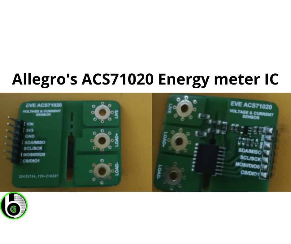
In many applications, we want to monitor AC electrical parameters like Solar chargers, motor control, Battery Charging stations, or Smart energy meters. Measurement of AC current and voltage, by the means of the electronics, is a quite tricky part, unlike traditional electromechanical systems. Below is a basic block diagram to know about it. AC voltage and current signals are first steps down to low voltage and current values.One can not feed High AC electrical voltage and Current signals which can range from 0-1000 units and are even larger than that, in some applications(Power systems, AC motors and etc) to the electronics and digital world. So at first by the use of one of the below listed three methods AC signals are brought to low values( 0-10V, 0-5A) Use of Current Transformer, Potential Transformer, or Rogowski coil. Use of shunt resistors. Use of Hall effect-based principal for current measurement. The signals which we get after processing from these methods are fed into the Digital System where there are signal conditioning circuits, data acquisition circuits, digital signal processing by the use of Digital and Analog Electronics. The Digital System part is designed to embedded into the Integrated chips(ASIC) which are specially designed with the purpose of Energy Metering application. For the digital computation of key electrical parameters like Power factor, Active power, reactive power, Vrms, Irms and etc. Using these key parameters we can monitor the AC electrical parameters through serial interfaces like SPI/I2C with Host MCU. ACS71020 Energy Metering IC Allegro microsystem\’ AC power monitor module ACS71020 is a Single-phase energy monitoring IC that works on the principle of the HALL effect sensing technique (To know about ways to measure current refer to this blog) to measure the AC current and resistor divider network to measure the input AC voltage. It calculates the key electrical parameters using its Metrology Engine and digital system from which it sends the data to the host MCU via I2C and SPI interfaces. The Voltage and current reading that we get from AC voltage and Current measurement blocks via the sense amplifiers are analog in nature. The analog signals from respective Voltage and Current blocks are then fed into the internal ADC\’s(Analog to Digital converter). ADC samples the current and voltage channels at high frequency and then digitally converts them by filtering and decimating the output signal from sense amplifiers to avoid large anti-aliasing filters. The digital word from the ADC is 16 bits for both the current and voltage, which is fed to the digital system for further calculation of other electrical parameters. Its Key Features are: Without the need for any Transformer, Rogowski coils, oversized current transformers, or the power loss of shunt resistors one can calculate Vrms and Irms up to 517V and 90A respectively It has an advanced digital system with galvanically isolated current sensing technology which achieves reinforced isolation ratings in a small PCB footprint Apart from the calculation of Electrical Key parameters it also has many extra features too which are essential for monitoring purposes. ACS71020 IC Pinout Diagram and Pins description ACS71020 IC has 16 pins, Starting from Pin 1-8 are current channel pins, out of which pins 1-4(Fused internally) are all IP+ and pins 5-8(fused internally) are all IP-. Pins 16-15 are Voltage measurement pins ACS71020 IC Schematic For using ACS71020 for typical applications its schematic is pretty easy and less complicated in oppose to other metering IC\’s(STMP32 & ADE series). ACS71020 can be powered directly from the same supply as the system\’s MCU, through its reinforced isolation technology it does need multiple power supplies to power it up. So Vcc and GND pins are connected directly to MCU Vcc and GND pins. I2C pins are at a high level(5V or 3v3), before the start of the I2C Serial Communication, thus SDA and SCL lines are connected with a pull-up resistor. When using in I2C mode, pins 9 & 10 act as DIO_1 and DIO_0( Digital Input/Output) respectively, which are connected directly to MCU Digital Pins( Will get in detail about DIO pins in a later section) For SPI communication, MOSI, MISO, CE pin are at a high level and CLK is at GRND before the start of SPI serial Communication. When using in SPI mode, pins 9 &10 are used as MOSI and CS pins. ACS71020 IC measures the Current and voltage of the input AC signal to calculate all other key parameters. So for inputting the AC voltage & current signals to the ACS71020 IC we will focus on Voltage channel pins(VINP & VINN) and Current channel pins(IP+ & IP-). One thing to recall is that in a single-phase AC supply there are two terminals: Live Wire (Black/Red) carries electricity from the power supply and takes it to the load. Neutral wire(Blue wire) returns the electricity from the load to the power supply to make the circuit complete. VINN &VINP are terminals from where AC voltage is measured, so resistor network divider of 1mega ohm and shunt resistor is made in b/w the VINP and VINN terminals to fit the input AC voltage within the Range of the differential voltage input buffer of ACS71020( +-275mv) as specified in electrical characteristics of the datasheet. IP+[1:4] & IP-[5-8] pins are terminals for AC current measurement. IP+ terminals are fused internally and are connected to a neutral wire of load and IP- terminals are also fused internally and are connected to a neutral wire of supply to complete the current loop of the current channel. EVE ACS71020 Module For doing the practical demonstration with ACS71020 IC we are going to use the EVE ACS71020 breakout board, which is manufactured by the Evelta. The module is cheap and can be used easily with HOST MCU via I2C or SPI communication. The module has pull-up resistors of 10k ohm placed with SDA and SCL pins( pins 12 & 11) of ACS71020 and no pull-up resistors are connected with MOSI and CS pins(pins 10 & 9) means we can use these
- 1
- 2