


Interfacing with the ElecronicsV2 Development Board
In previous blog we covered a brief overview of how the OLED display works in microscopic level and also understood various types of OLED displays available in the market . In this blog we’ll be discussing how to configure the SSD1306 display with the microcontroller and we’ll be making the embedded driver as well.128×64 display is a dot matrix display , hence 128×64 =8192 total pixels . It is by turning on/off these pixels we display graphical image of any shape . It is the current provided to each pixel that varies the brightness. HARDWARE DESCRIPTION OLED Display chosen is driven by SSD1306 Driver IC although they are other ICs such as SSD1331 which can be used to drive the display . These ICs are CMOS OLED Driver controller for dot-matrix system . OLED has 256 brightness steps .Besides 128×64 , 128×32 display resolution is also available. Specification of ssd1306 128×64 OLED Display Type: OLED (Organic Light Emitting Diode) Display Size: 128×64 pixels Display Driver: ssd1306 Display Colors: Monochrome (White), Yellow, and Blue Operating Voltage: 3.3V to 5V Interface: I2C Operating Current: ~20mA Display Structure OLED DISPLAY is mapped using GDDRAM page structure OF SSD1306 GDDRAM or graphic display ram is a bit mapped static RAM . It holds the bit pattern to be displayed. The GDDRAM having size 128×64 is divided into 8 pages from PAGE 0 TO PAGE 7 which is used for monochrome matrix display . When data bit D0 – D7 is sent the row0 gets filled with D0 and D7 is written into the bottom row. Display has 64 rows , 128 columns divided into 8 pages . Each page has 128 columns and 8 rows. Display 128 columns known as segments For displaying the graphical data in the first location , page address and column address both are set to 0 with the end address of page and column also being selected End of column and End of the page is 7FH and 07H respectively SSD1306 BLOCK DIAGRAM PIN ARANGEMENT SSD1306 FUNCTIONAL BLOCK DIAGRAM SSD1306 BLOCK DIAGRAM PIN ARANGEMENT SSD1306 FUNCTIONAL BLOCK DIAGRAM ADDRESSING MODE 1. PAGE ADDRESSING MODE 2.Horizontal Addressing Mode 3.Vertical Addressing Mode 1. PAGE ADDRESSING MODE In page addressing mode, after the display RAM is read/written, the column address pointer is increased automatically by 1. If the column address pointer reaches column end address, the column address pointer is reset to column start address but page address pointer not points to next page. Hence, we need to set the new page and column addresses in order to access the next page RAM content. We need to set lower two bits to ‘1’ and ‘0’ for Page Addressing Mode. In page addressing mode, the following steps are required to define the starting RAM access pointer location: Set the page start address of the target display location by command B0h to B7h. Set the lower start column address of pointer by command 00h~0Fh. Set the upper start column address of pointer by command 10h~1Fh 2.Horizontal Addressing Mode In horizontal addressing mode, after the display RAM is read/written, the column address pointer is increased automatically by 1. If the column address pointer reaches column end address, the column address pointer is reset to column start address and page address pointer is increased by 1. When both column and page address pointers reach the end address, the pointers are reset to column start address and page start address We need to set last two digits to ‘0’ and ’0’ for horizontal addressing mode. 3.Vertical Addressing Mode In vertical addressing mode, after the display RAM is read/written, the page address pointer is increased automatically by 1. If the page address pointer reaches the page end address, the page address pointer is reset to page start address and column address pointer is increased by 1. When both column and page address pointers reach the end address, the pointers are reset to column start address and page start address. We need to set last two digits to ‘0’ and ’1’ for vertical addressing mode. In normal display data RAM read or write and horizontal/vertical addressing mode, the following steps are required to define the RAM access pointer location: Set the column start and end address of the target display location by command 21h. Set the page start and end address of the target display location by command 22h. Hardware Pinout SDAThis pin is used to send data between master and slave with the acknowledgement of the master SCLThis is a clock signal that helps keeps the process in synchronization VCCA power supply of 3.3 V is required . More than 3.3V may damage the module GNDThis ground pin is connected to the ground supply ALGORITHM Select the I2C slave address and specify the operation that will be performed i.e Read 0x79 or Write 0x78. #define SSD1306_I2C_ADDR 0x78 Set the clock divide ratio and oscillator frequency . Bit 3-0 sets the clock divide ratio , Bit 7-4 sets the oscillator frequency SSD1306_WRITECOMMAND(0xD5); //–set display clock divide ratio/oscillator frequency SSD1306_WRITECOMMAND(0xF0); //–set divide ratio Set the multiplex ratio switching to any value ranging from 16-63 SSD1306_WRITECOMMAND(0xA8); //–set multiplex ratio(1 to 64) Display start line addressing in which the starting address of the display ram is determined . In our case this is set to zero and RAM row 0 is mapped to col 0 SSD1306_WRITECOMMAND(0x40); //–set start line address Set memory addressing mode using page addressing mode, horizontal addressing mode, vertical addressing mode. SSD1306_WRITECOMMAND(0x10); //00,Horizontal Addressing Mode;01,Vertical Addressing Mode;10,Page Addressing Mode (RESET);11,Invalid SSD1306_WRITECOMMAND(0xB0); //Set Page Start Address for Page Addressing Mode,0-7 Set column address using a triple byte first specifies the column setting , second column start and third column end . Do the same for the page SSD1306_WRITECOMMAND(0x00); //—set low column address SSD1306_WRITECOMMAND(0x10); //—set high column address Set pre-charge period and VCOMH deselect level SSD1306_WRITECOMMAND(0xDB); //–set vcomh Entire display is on using A4H and A5H command SSD1306_WRITECOMMAND(0xA4); //0xa4,Output follows RAM content;0xa5,Output ignores RAM content The normal functionality of the
Display Technolgy mainly consists of two things: Display Devices and Display Driver Integrated Chips(DDIC). Display Devices: are OLED, LCD, LED, CRT, Vacuum Florescent, etc modules. To know in-depth about the different types of display devices refer to this. Display Driver Integrated Chips(DDIC): are semiconductor IC\’s that provide an interface between the control Unit(MPU and MCU) and a particular type of display device. Display driver accepts commands and data using onboard communication protocols like I2C, SPI, CMOS, RS232, etc and generates signals with suitable voltage, current, timing, and demultiplexing to make the display show the desired text or image. Display driver IC\’s may also incorporate RAM, Flash Memory, EEPROM, and/or ROM. Examples of Display Driver IC are SSD1306, HD44780, KS0108, SSD1815, and ST7920. In this blog, we are going to use the OLED Display device and will go in-depth into one of the OLED Display Driver IC\’s: SSD1306 by Solomon Systech. OLED Display Introduction OLED(Organic Light Emitting Diode) displays are the new technology in the display screen industry that are revolutionizing the user interface for users in various devices like TV screens, Virtual Reality headsets, Smart Watches, and many more. LCD Technology is compentator to OLED technology. LCD is a non-emission and older display technology that requires an external light source to work. While OLED technology is modern and considered to be emission display technology, that does not require a backlight that is an external light source. OLED Display technology is pretty exciting and opens lots of possibilities: Curved OLED Display Wearable OLED\’s Flexible and rollable OLED Transparent OLED embedded in Windows and many more we can not imagine today. The focus of this blog will be more on the understanding of OLED Display Driver IC: SSD1306 and its driver development for operating the below OLED Screen Module. To get to know about the OLED display working and its layers, readers can refer to this blog. OLED Driver IC\’s apart from SSD1306 are SSD0323. SSD1306 OLED Driver IC SSd1306 is an integrated chip that is used to drive the OLED display of the dot-matrix graphic display system. These IC\’s comes in Chip on glass or Chip on Film packaging i.e chip die is directly mounted to a piece of the glass display. SSD1306 has a feature to drive up to 128 columns & 64 rows of OLED pixels. It has constant control, display RAM and oscillator inbuilt which reduces the external components and power consumption. SSD1306 IC itself require only 1.65 to 3.3 V that can be provided to it easily from MCU. But as OLED displays does not have backlight as LCD has, so the panel of OLED requires higher voltages of about 7-15 V which is supplied to OLED panel from internal voltage doublers and charge pump circuitry\’s. And on an average OLED display consumes only 20mA current. Now coming to the part that how does these Driver IC display data on these OLED screens.
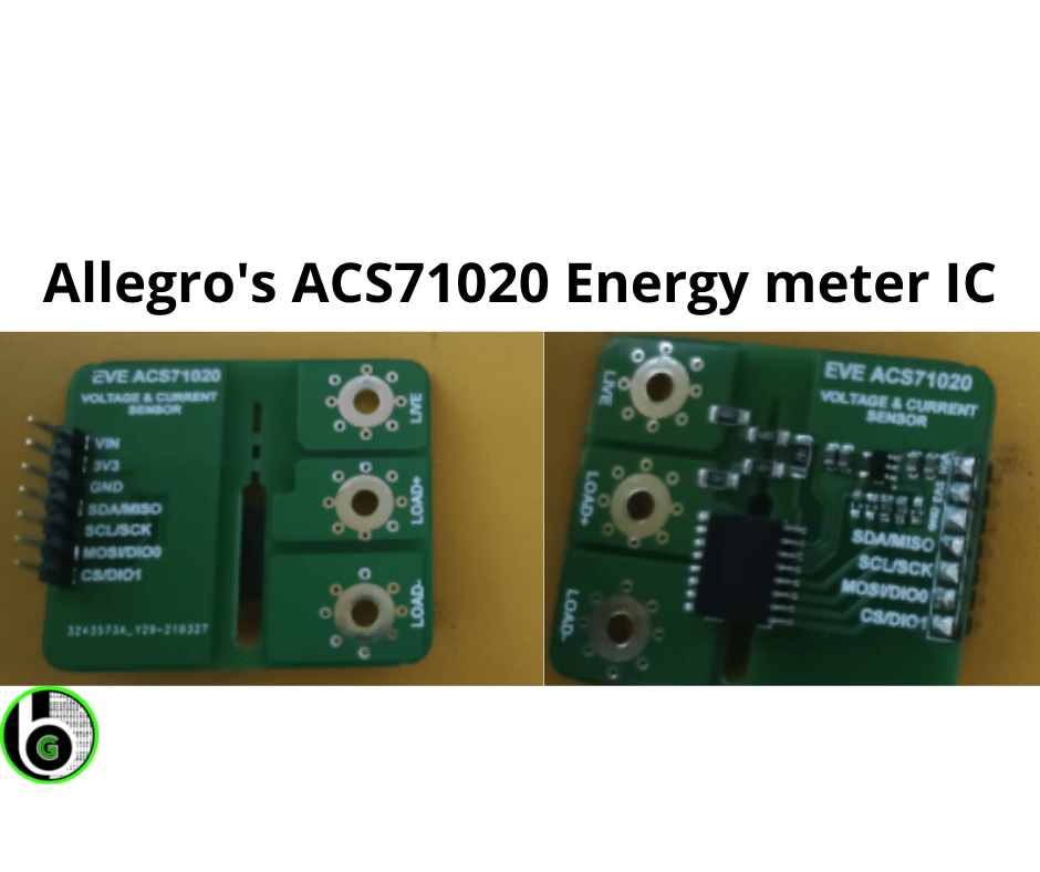
In many applications, we want to monitor AC electrical parameters like Solar chargers, motor control, Battery Charging stations, or Smart energy meters. Measurement of AC current and voltage, by the means of the electronics, is a quite tricky part, unlike traditional electromechanical systems. Below is a basic block diagram to know about it. AC voltage and current signals are first steps down to low voltage and current values.One can not feed High AC electrical voltage and Current signals which can range from 0-1000 units and are even larger than that, in some applications(Power systems, AC motors and etc) to the electronics and digital world. So at first by the use of one of the below listed three methods AC signals are brought to low values( 0-10V, 0-5A) Use of Current Transformer, Potential Transformer, or Rogowski coil. Use of shunt resistors. Use of Hall effect-based principal for current measurement. The signals which we get after processing from these methods are fed into the Digital System where there are signal conditioning circuits, data acquisition circuits, digital signal processing by the use of Digital and Analog Electronics. The Digital System part is designed to embedded into the Integrated chips(ASIC) which are specially designed with the purpose of Energy Metering application. For the digital computation of key electrical parameters like Power factor, Active power, reactive power, Vrms, Irms and etc. Using these key parameters we can monitor the AC electrical parameters through serial interfaces like SPI/I2C with Host MCU. ACS71020 Energy Metering IC Allegro microsystem\’ AC power monitor module ACS71020 is a Single-phase energy monitoring IC that works on the principle of the HALL effect sensing technique (To know about ways to measure current refer to this blog) to measure the AC current and resistor divider network to measure the input AC voltage. It calculates the key electrical parameters using its Metrology Engine and digital system from which it sends the data to the host MCU via I2C and SPI interfaces. The Voltage and current reading that we get from AC voltage and Current measurement blocks via the sense amplifiers are analog in nature. The analog signals from respective Voltage and Current blocks are then fed into the internal ADC\’s(Analog to Digital converter). ADC samples the current and voltage channels at high frequency and then digitally converts them by filtering and decimating the output signal from sense amplifiers to avoid large anti-aliasing filters. The digital word from the ADC is 16 bits for both the current and voltage, which is fed to the digital system for further calculation of other electrical parameters. Its Key Features are: Without the need for any Transformer, Rogowski coils, oversized current transformers, or the power loss of shunt resistors one can calculate Vrms and Irms up to 517V and 90A respectively It has an advanced digital system with galvanically isolated current sensing technology which achieves reinforced isolation ratings in a small PCB footprint Apart from the calculation of Electrical Key parameters it also has many extra features too which are essential for monitoring purposes. ACS71020 IC Pinout Diagram and Pins description ACS71020 IC has 16 pins, Starting from Pin 1-8 are current channel pins, out of which pins 1-4(Fused internally) are all IP+ and pins 5-8(fused internally) are all IP-. Pins 16-15 are Voltage measurement pins ACS71020 IC Schematic For using ACS71020 for typical applications its schematic is pretty easy and less complicated in oppose to other metering IC\’s(STMP32 & ADE series). ACS71020 can be powered directly from the same supply as the system\’s MCU, through its reinforced isolation technology it does need multiple power supplies to power it up. So Vcc and GND pins are connected directly to MCU Vcc and GND pins. I2C pins are at a high level(5V or 3v3), before the start of the I2C Serial Communication, thus SDA and SCL lines are connected with a pull-up resistor. When using in I2C mode, pins 9 & 10 act as DIO_1 and DIO_0( Digital Input/Output) respectively, which are connected directly to MCU Digital Pins( Will get in detail about DIO pins in a later section) For SPI communication, MOSI, MISO, CE pin are at a high level and CLK is at GRND before the start of SPI serial Communication. When using in SPI mode, pins 9 &10 are used as MOSI and CS pins. ACS71020 IC measures the Current and voltage of the input AC signal to calculate all other key parameters. So for inputting the AC voltage & current signals to the ACS71020 IC we will focus on Voltage channel pins(VINP & VINN) and Current channel pins(IP+ & IP-). One thing to recall is that in a single-phase AC supply there are two terminals: Live Wire (Black/Red) carries electricity from the power supply and takes it to the load. Neutral wire(Blue wire) returns the electricity from the load to the power supply to make the circuit complete. VINN &VINP are terminals from where AC voltage is measured, so resistor network divider of 1mega ohm and shunt resistor is made in b/w the VINP and VINN terminals to fit the input AC voltage within the Range of the differential voltage input buffer of ACS71020( +-275mv) as specified in electrical characteristics of the datasheet. IP+[1:4] & IP-[5-8] pins are terminals for AC current measurement. IP+ terminals are fused internally and are connected to a neutral wire of load and IP- terminals are also fused internally and are connected to a neutral wire of supply to complete the current loop of the current channel. EVE ACS71020 Module For doing the practical demonstration with ACS71020 IC we are going to use the EVE ACS71020 breakout board, which is manufactured by the Evelta. The module is cheap and can be used easily with HOST MCU via I2C or SPI communication. The module has pull-up resistors of 10k ohm placed with SDA and SCL pins( pins 12 & 11) of ACS71020 and no pull-up resistors are connected with MOSI and CS pins(pins 10 & 9) means we can use these