Introduction
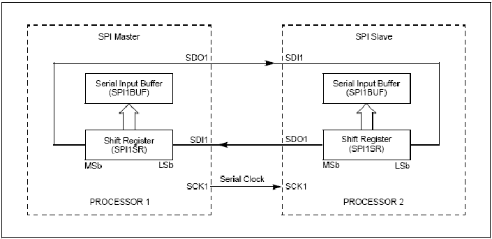
–> SPI (Serial Peripheral Interface) is one of microcontrollers’ most widely used communication protocols. For a concise and beginner-friendly explanation of SPI communication as a concept, check out this BLOG. It will give you a foundational understanding in just a few minutes. SPI is commonly used in devices like SD cards, sensors, and display modules:
- SD Cards – SPI is used for high-speed data transfer in storage applications.
- Sensors (e.g., MPU6050, BME280) – These devices use SPI to send real-time data such as acceleration, pressure, and temperature.
- Display Modules (e.g., OLED, TFT) – SPI facilitates fast graphics and text rendering on screens.
–> In the S32K144 microcontroller, the SPI peripheral is called LPSPI (Lower-Power Serial Peripheral Interface), offering additional features and advanced configuration compared to standard SPI modules.
- Low CPU Overhead: With FIFO registers and DMA support, LPSPI minimizes CPU involvement by offloading register access tasks. This makes it ideal for applications requiring efficient and high-speed data handling.
–> NOTE: A single SPI communication setup typically involves four main signals: MOSI (Master Out, Slave In), MISO (Master In, Slave Out), CLK (Clock), and CS (Chip Select).
–> The table below highlights the available SPI instances in different series of microcontrollers, with specific emphasis on our development board.

Features of SPI
–> The LPSPI module offers a variety of advanced features for versatile and efficient communication. Let’s group and explain these features:
1. Data Configuration and Flexibility
- Word Size (32 bits): LPSPI can handle data packets of up to 32 bits, allowing flexibility in the amount of data exchanged during communication.
- Full Duplex and Half Duplex Transfers:
- Full Duplex(4-wire SPI): Simultaneous data transmission and reception, supporting 1-bit data transfer per clock edge.
- Half Duplex(3-wire SPI): Allows for either transmitting or receiving on each clock edge, supporting different configurations:
- 1-bit, 2-bit, or 4-bit transfers: Multiple bits can be sent or received per clock cycle, enhancing data transfer speed in master mode.

2. Clock Configuration and Timing Control
- Configurable Clock Polarity and Phase: Adjusting these settings ensures compatibility with various SPI devices by controlling how data aligns with clock edges.
- Master Timing Flexibility: In master mode, it allows control over:
- Clock (SCK) Frequency: Adjusting speed for optimal communication.
- Delays: Fine-tuning the timing between chip select (PCS) and clock (SCK) edges for synchronization.

3. Operating Modes
- Master and Slave Operations:
- Master: Controls the SPI bus and initiates data transfers, supporting up to 4 chip selects for connecting multiple devices.
- Slave: Responds to commands from the master, enabling versatile device interactions.
- Master and Slave Operations:

4. Buffer and Data Handling
- Command/Transmit and Receive FIFOs (4 words each): Buffers that hold up to 4 words of data for efficient handling of transmit and receive operations, reducing CPU workload.
- Receive Data Match Logic: Matches specific data patterns to trigger a wakeup event, useful for low-power applications.

5. Additional Features
- Host Request Support (Master Only): Allows external control to start SPI transfers, adding flexibility in managing bus communication.
- Multiple Chip Selects: Supports up to 4 peripherals using individual chip select lines for efficient control of multiple slave devices.

