In this blog we are going to explore the SPI Peripheral. Going to Start with SPI peripheral. Objective would be to get.
familiarity with SPI peripheral for S32K144 MCU.
Would be understanding SPI peripheral from Hardware point of view in S32K144 MCU.
Going to understand then how to use SPI peripheral via S32K SDK/lpspi driver.
Would also be demonstrating the spi_echo_pall sketch.
So read along the blog and do tell me its reviews
SPI Peripheral Theory
Serial Peripjeral interface is a synchronous serial communication interface used in embedded systems, typically to perform short distance communications between microcontrollers and device. Typical applications include interfacing to LCD displays, memory cards, Secure Digital cards and etc.
SPI Peripheral in S32K144 MCU
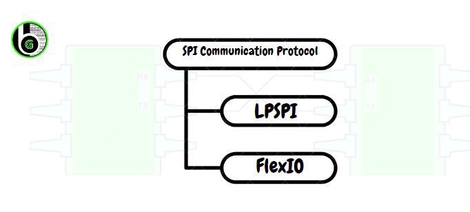
In S32K144 MCU, SPI protocol can be used via 2 peripherals: LPSPI & FlexIO.
SPI protocol in S32K144
LPSPI is referred as Low Power Serial Peripheral Interface. LPSPI is on chip peripheral only to do SPI communication protocol. SPI is a serial protocol which is done via SPI supported peripherals in the Microcontrollers.
Also, in S32K144 there is FlexIO peripheral through which on-board serial communication protocols like UART, I2C & SPI can be emulated. So through FlexIO peripheral, also SPI peripheral can be implemented. To know about FlexIO peripheral in S32K144, refer to this blog.
Features of SPI via LPSPI peripheral in S32K144 MCU:
LPSPI module supports efficient interface to an SPI bus, as a master and slave.
LPSPI is designed to use little CPU overhead, with DMA support. LPSPI can generate a DMA request.
SPI devices communicate in full duplex mode using a master-slave scheme, with a single master at a time.
Single master can control multiple slave devices using individual slave select (SS) lines.
If MCU is configured as Master, then it will generate the frame for reading and wiriting and SPI clock which is synchronous.
Supports daisychain for controlling multiple slave sharing the same chip select.
Configurable clock polarity and clock phase
Master operation supporting upto 4 peripheral chip selects at a time
Transmit and receive FIFO of 4 words for both master and slave device.
Flexible timing parameters in master mode, including SCK frequency and delays between PCS and SCK edges.
Support for Full duplex transfers, supporting 1 bit transfers and receive on each clock edge.
Support for full-duplex transfers, supporting 1-bit/2-bit/4-bit transfers and receive on each clock edge.
How to get started with I2C peripheral in S32K144 MCU
SPI Hardware Pinout in S32K144 MCU
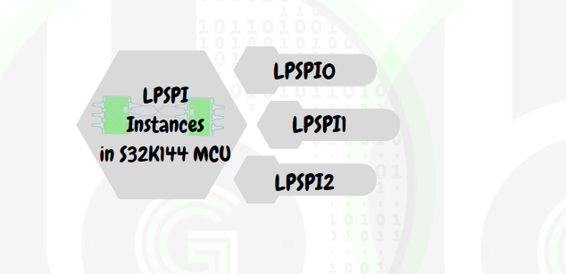
LPSPI Pinout and Hardware Instances
LPSPI peripheral in S32K144 has 3 instances: LPSPI0, LPSPI1, LPSPI2.
LPSPI Instances in S32K144 MCU
In S32K MCU, LPSPI peripheral can be used in serial and parallel data transfers. For this blog we are going to focus on serial data transfers. to know about parallel data transfers, refer to this blog.
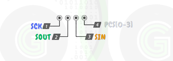
All the LPSPI instances has following pins, for using them.
SCK (Serial clock): This pin is used to generate the clock pulses in SPI communication by the Master.
SOUT (Serial data out): This pin is MOSI pin.
SIN (Serial Data Input): This pin is MISO pin.
PCS [0] (Peripheral Chip Select 0): This pin is used to select the slave in SPI communication. Master device will generate a Low Signal on this Pin to select the Slave. And generate High signal to deselect the Slave.
For SOUT there are 3 pinsLPSPI0 pins in S32K1443 pins.
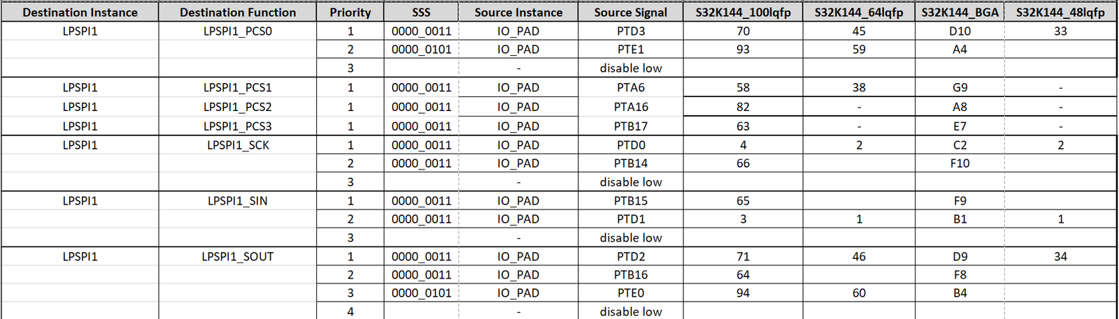
LPSPI1
In LPSPI1 there are following number of pins:
For PCS0 there are 2 pins
For PCS1 there is 1 pin.
For PCS2 there is 1 pin.
For PCS3 there is 1 pin.
For SCK there are 2 pins
For SIN there are 2 pins.
For SOUT there are 3 pins.
LPSPI1 pins in S32K144
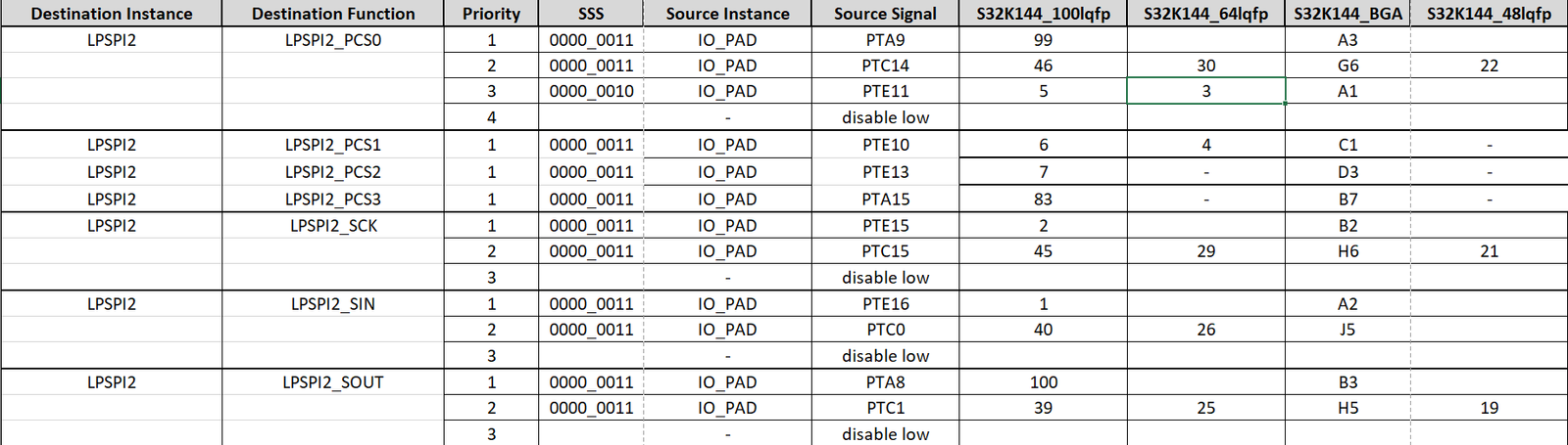
LPSPI2
In LPSPI2 there are following number of pins:
For PCS0 there are 3 pins
For PCS1 there is 1 pin.
For PCS2 there is 1 pin.
For PCS3 there is 1 pin.
For SCK there are 2 pins
For SIN there are 2 pins.
For SOUT there are 2 pins.
LPSPI2 pins in S32K144 MCU
How to do LPSPI Pin Configuration
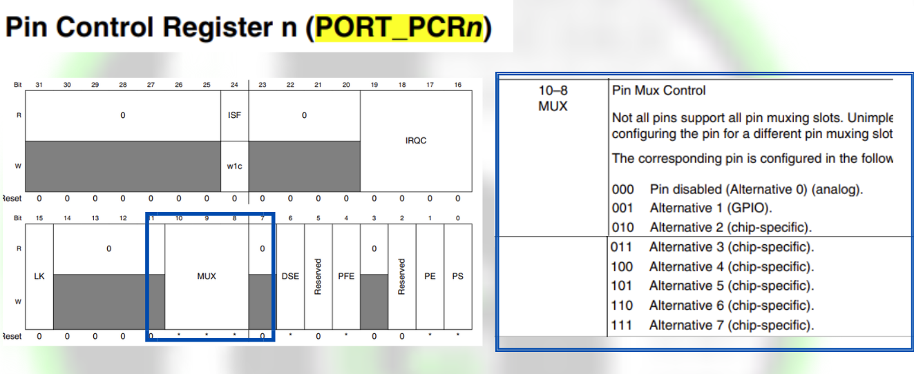
In a MCU a single pin can work as multiple function, so we have to configure that which function we need, accordingly pins have to be configured. This configuration of Alternate functions of pins in S32K144 MCU is done by Signal Multiplexing peripheral. One can configure which pin to use for LPI2C, via Signal Multiplexing peripheral, in which there is a register Pin Control Register (PCR) which has Pin Mux Control bits(MUX) for configuring the alternate functions of the pins.
PCR register of S32K144
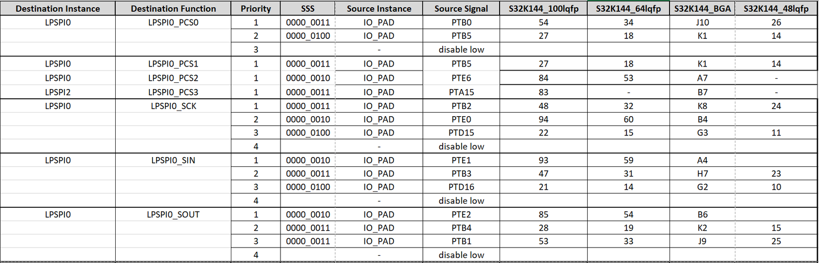
For example, we are using LPISPI0. Now in LPISPI0 for using LPSPI0_PCS0, LPSPI0_SCK, LPSPI0_SOUT, LPSPI0_SIN pins one can configure PTB0, PTB2, PTB4, PTE1 pins:
You can see SSS column in the excel in that for PTB0 under LPSPI0_PCS has value of 0000_0011. Last 3 bits of this value represents the MUX values to be configured for configuring PTB0 pin as LPSPI0_PCS pin, in PORT_PCRn register.
You can see SSS column in the excel in that for PTB2 under LPSPI0_SCKhas value of 0000_0011. Last 3 bits of this value represents the MUX values to be configured for configuring PTB2 pin as LPSPI0_SCK pin, in PORT_PCRn register.
You can see SSS column in the excel in that for PTB4 under LPSPI0_SOUT has value of 0000_0011. Last 3 bits of this value represents the MUX values to be configured for configuring PTB4 pin as LPSPI0_SOUT pin, in PORT_PCRn register.
You can see SSS column in the excel in that for PTE1 under LPSPI0_SCKhas value of 0000_0010. Last 3 bits of this value represents the MUX values to be configured for configuring PTE1 pin as LPSPI0_SIN pin, in PORT_PCRn register.
This part of LPSPI pins configuration is done internally by S32 SDK/pin driver (Its detail overview is in GPIO Peripheral in S32K144 MCU). When writing the code, we just need to configure the structure g_pin_InitConfig in which. mux member for the corresponding MCU pin will be assigned value according to last 3 bits of SSS column, as shown below and pass that structure in PINS_DRV_Init().
At line 12, 25, 38, 51 you see .mux is assigned with PORT_MUX_ALT_3 & PORT_MUX_ALT_2. The value of this is taken from port_mux_t Enum which is defined in pins_driver.h file as follows. The members defined in this Enum is according to the MUX bits values defined in PCRn register. So according to the value of the last 3 bits of SSS column, we will configure the. mux member of g_pin_InitConfig structure
					/*!
 * @brief Configures the Pin mux selection
 * Implements : port_mux_t_Class
 */
typedef enum
{
    PORT_PIN_DISABLED            = 0U,  /*0b000!< corresponding pin is disabled, but is used as an analog pin       */
    PORT_MUX_AS_GPIO             = 1U,  /*0b001!< corresponding pin is configured as GPIO                           */
    PORT_MUX_ALT2                = 2U,  /*0b010!< chip-specific                                                     */
    PORT_MUX_ALT3                = 3U,  /*0b011!< chip-specific                                                     */
    PORT_MUX_ALT4                = 4U,  /*0b100!< chip-specific                                                     */
    PORT_MUX_ALT5                = 5U,  /*0b101!< chip-specific                                                     */
    PORT_MUX_ALT6                = 6U,  /*0b110!< chip-specific                                                     */
    PORT_MUX_ALT7                = 7U,  /*0b111!< chip-specific                                                     */
#if FEATURE_PINS_HAS_ADC_INTERLEAVE_EN
    PORT_MUX_ADC_INTERLEAVE      = 8U   /*!< when selected, ADC Interleaved channel is connected to current pin
                                         *   and disconnected to opposed pin
                                         * ADC1_SE14-PTB15 | ADC1_SE15-PTB16 | ADC0_SE8-PTC0  | ADC0_SE9-PTC1
                                         * ADC1_SE14-PTB0  | ADC1_SE15-PTB1  | ADC0_SE8-PTB13 | ADC0_SE9-PTB14 */
#endif /* FEATURE_PINS_HAS_ADC_INTERLEAVE_EN */
} port_mux_t;
SPI SDK in S32K144 MCU
LPSPI SDK
S32K SDK/drivers provide an easy to use and quick way to use the LPI2C peripheral in S32K144, which is known as LPSPI SDK.
LPSPI SDK for S32K144 MCU
Each S32 SDK driver can be configured and enabled to use in the project via S32 Configuration Tool. Will be digging into that part, in next section. For now, let’s understand the LPSPI SDK in some detail, so as to use SPI peripheral via LPSPI.
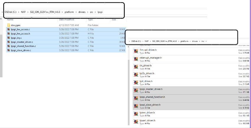
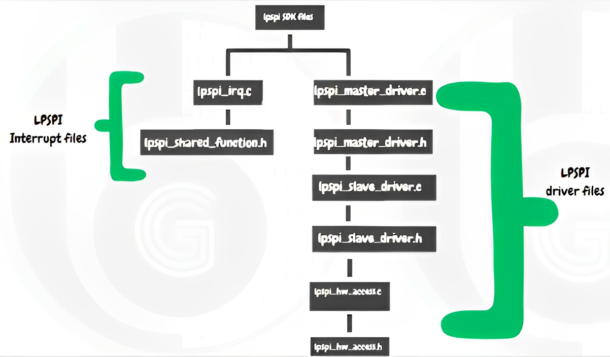
LPSPI interrupt files contains functions for using &configuring of LPSPI interrupts and some common functions that has to be used by both master and slave
LPSPI driver filescontains functions for using/configuration of LPSPI Peripheral.
LPSPI Driver
LPI2C driver files are further divided into LPI2C Peripheral Abstraction Layer(PAL) & LPI2C Low Level drivers, as shown below:
LPSPI Driver files
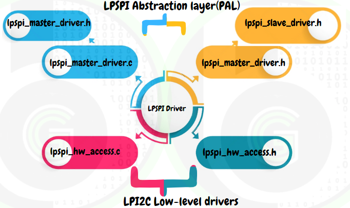
LPSPI Peripheral Abstraction Layer (PAL): contains functions and variables that are directly used in main.c or application code. And internally these functions use the LPSPI Low-level drivers & LPSPI IRQ. So if hardware is changed LPSPI PAL would remain same and only internal low-level driver files need to be changed or modified. By this way we don’t have make many changes on application level.
LPSPI Low-level driver: contains functions that configures the LPSPI peripheral registers for initializing the peripheral, using the peripheral and processing the data of peripheral at hardware level. These files are the ones which actually interacts with the hardware and make it configurable to our needs. Flow to use LPSPI peripheral in S32K144 MCU
In the blogs we will be exploring the LPSPI Peripheral Abstraction Layer files (PAL) in more details, as that would be directly used in our application project development(main.c) and driver creation of I2C modules (Display Screens, Memory Cards and IoT Modules
LPSPI PAL
In LPSPI PAL their are 4 files, 2 files for SPI master and 2 files for SPI Slave.
Let’s get into these files:
lpspi_master_driver.h & lpspi_slave_driver.h: Contains the Enum’s, structures and function declarations that would be used in application code. Only functions which are declared in these header files can be used in main.c or application project.
lpspi_master_driver.c & lpspi_slave_driver.c: Contains the function definitions of the declared functions (uses the low-level driver functions) along with some static functions also that are restricted to use in this file only.
Functions
LPSPI Master Functions
LPSPI_DRV_MasterInit: This function is first function to be used in main.c or application code to initialize the SPI peripheral in Master Mode.
Lorem ipsum dolor sit amet, consectetur adipiscing elit. Ut elit tellus, luctus nec ullamcorper mattis, pulvinar dapibus leo.
console.log( 'Code is Poetry' );
LPSPI Master data Types
Their are 2 structures that are important and will be used:
lpspi_master_config_t: This structure has members to configure the LPSPI Master according to user defined settings.
					/*!
 * @brief Data structure containing information about a device on the SPI bus.
 *
 * The user must populate these members to set up the LPSPI master and
 * properly communicate with the SPI device.
 * Implements : lpspi_master_config_t_Class
 */
typedef struct
{
    uint32_t bitsPerSec;                 /*!< Baud rate in bits per second*/
    lpspi_which_pcs_t whichPcs;          /*!< Selects which PCS to use */
    lpspi_signal_polarity_t pcsPolarity; /*!< PCS polarity */
    bool isPcsContinuous;                /*!< Keeps PCS asserted until transfer complete */
    uint16_t bitcount;                   /*!< Number of bits/frame, minimum is 8-bits */
    uint32_t lpspiSrcClk;                /*!< Module source clock */
    lpspi_clock_phase_t clkPhase;        /*!< Selects which phase of clock to capture data */
    lpspi_sck_polarity_t clkPolarity;    /*!< Selects clock polarity */
    bool lsbFirst;                       /*!< Option to transmit LSB first */
    lpspi_transfer_type transferType;    /*!< Type of LPSPI transfer */
    uint8_t rxDMAChannel;                /*!< Channel number for DMA rx channel. If DMA mode isn't used this field will be ignored. */
    uint8_t txDMAChannel;                /*!< Channel number for DMA tx channel. If DMA mode isn't used this field will be ignored. */
    spi_callback_t callback;             /*!< Select the callback to transfer complete */
    void *callbackParam;                 /*!< Select additional callback parameters if it's necessary */
} lpspi_master_config_t;
Tab #1
Tab #2
Tab #1
Lorem ipsum dolor sit amet, consectetur adipiscing elit. Ut elit tellus, luctus nec ullamcorper mattis, pulvinar dapibus leo.
Tab #2
Lorem ipsum dolor sit amet, consectetur adipiscing elit. Ut elit tellus, luctus nec ullamcorper mattis, pulvinar dapibus leo.
lpspi_state_t: This structure has data members, which keep track of the on-going transfers .
					/*!
 * @brief Runtime state structure for the LPSPI master driver.
 *
 * This structure holds data that is used by the LPSPI peripheral driver to
 * communicate between the transfer function and the interrupt handler. The
 * interrupt handler also uses this information to keep track of its progress.
 * The user must pass  the memory for this run-time state structure. The
 * LPSPI master driver populates the members.
 * Implements : lpspi_state_t_Class
 */
typedef struct
{
    uint16_t bitsPerFrame;               /*!< Number of bits per frame: 8- to 4096-bits; needed for
                                              TCR programming */
    uint16_t bytesPerFrame;              /*!< Number of bytes per frame: 1- to 512-bytes */
    bool isPcsContinuous;                /*!< Option to keep chip select asserted until transfer
                                              complete; needed for TCR programming */
    bool isBlocking;                     /*!< Save the transfer type */
    uint32_t lpspiSrcClk;                /*!< Module source clock */
    volatile bool isTransferInProgress;  /*!< True if there is an active transfer */
    const uint8_t * txBuff;                      /*!< The buffer from which transmitted bytes are taken */
    uint8_t * rxBuff;                    /*!< The buffer into which received bytes are placed */
    volatile uint16_t txCount;           /*!< Number of bytes remaining to send  */
    volatile uint16_t rxCount;           /*!< Number of bytes remaining to receive */
    volatile uint16_t txFrameCnt;        /*!< Number of bytes from current frame which were already sent */
    volatile uint16_t rxFrameCnt;        /*!< Number of bytes from current frame which were already received */
    volatile bool lsb;                   /*!< True if first bit is LSB and false if first bit is MSB */
    uint8_t fifoSize;                    /*!< RX/TX fifo size */
    uint8_t rxDMAChannel;                /*!< Channel number for DMA rx channel */
    uint8_t txDMAChannel;                /*!< Channel number for DMA tx channel */
    lpspi_transfer_type transferType;    /*!< Type of LPSPI transfer */
    semaphore_t lpspiSemaphore;          /*!< The semaphore used for blocking transfers */
    transfer_status_t status;            /*!< The status of the current */
    spi_callback_t callback;             /*!< Select the callback to transfer complete */
    void *callbackParam;                 /*!< Select additional callback parameters if it's necessary */
    uint32_t dummy;                      /*!< This field is used for the cases when TX is NULL and LPSPI is in DMA mode */
} lpspi_state_t;
Tab #1
Tab #2
Tab #1
Lorem ipsum dolor sit amet, consectetur adipiscing elit. Ut elit tellus, luctus nec ullamcorper mattis, pulvinar dapibus leo.
Tab #2
Lorem ipsum dolor sit amet, consectetur adipiscing elit. Ut elit tellus, luctus nec ullamcorper mattis, pulvinar dapibus leo.
					/* Define state structure for current SPI instance */
lpspi_state_t lpspi_1State;
Lorem ipsum dolor sit amet, consectetur adipiscing elit. Ut elit tellus, luctus nec ullamcorper mattis, pulvinar dapibus leo.
console.log( 'Code is Poetry' );
LPSPI_DRV_SlaveIRQHandler
void LPSPI_DRV_SlaveIRQHandler(uint32_t instance)
Lorem ipsum dolor sit amet, consectetur adipiscing elit. Ut elit tellus, luctus nec ullamcorper mattis, pulvinar dapibus leo.
console.log( 'Code is Poetry' );
LPSPI Slave data Types
Their are 2 structures that are important and will be used:
lpspi_slave_config_t: This structure has members to configure the LPSPI Slave according to user defined settings.
					/*!
 *  @brief User configuration structure for the SPI slave driver.
 * Implements : lpspi_slave_config_t_Class
 */
typedef struct
{
    lpspi_signal_polarity_t pcsPolarity; /*!< PCS polarity */
    uint16_t bitcount;                   /*!< Number of bits/frame, minimum is 8-bits */
    lpspi_clock_phase_t clkPhase;        /*!< Selects which phase of clock to capture data */
    lpspi_which_pcs_t whichPcs;
    lpspi_sck_polarity_t clkPolarity;    /*!< Selects clock polarity */
    bool lsbFirst;                       /*!< Option to transmit LSB first */
    lpspi_transfer_type transferType;    /*!< Type of LPSPI transfer */
    uint8_t rxDMAChannel;                /*!< Channel number for DMA rx channel. If DMA mode isn't used this field will be ignored. */
    uint8_t txDMAChannel;                /*!< Channel number for DMA tx channel. If DMA mode isn't used this field will be ignored. */
    spi_callback_t callback;             /*!< Select the callback to transfer complete */
    void *callbackParam;                 /*!< Select additional callback parameters if it's necessary */
} lpspi_slave_config_t;
Tab #1
Tab #2
Tab #1
Lorem ipsum dolor sit amet, consectetur adipiscing elit. Ut elit tellus, luctus nec ullamcorper mattis, pulvinar dapibus leo.
Tab #2
Lorem ipsum dolor sit amet, consectetur adipiscing elit. Ut elit tellus, luctus nec ullamcorper mattis, pulvinar dapibus leo.
					/*
 * Copyright 2020 NXP
 * All rights reserved.
 *
 * NXP Confidential. This software is owned or controlled by NXP and may only be
 * used strictly in accordance with the applicable license terms. By expressly
 * accepting such terms or by downloading, installing, activating and/or otherwise
 * using the software, you are agreeing that you have read, and that you agree to
 * comply with and are bound by, such license terms. If you do not agree to be
 * bound by the applicable license terms, then you may not retain, install,
 * activate or otherwise use the software. The production use license in
 * Section 2.3 is expressly granted for this software.
 */
/*!
** @file main.c
** @brief
**         Main module.
**         This module contains user's application code.
*/
/*!
**  @addtogroup main_module main module documentation
**  @{
*/
/* MODULE main */


/* Including necessary configuration files. */
#include "sdk_project_config.h"

volatile int exit_code = 0;

/* User includes */
#include <stdint.h>
#include <stdbool.h>

#define TIMEOUT             1000U
#define NUMBER_OF_FRAMES    100U
#define RED_LED             (1<<15U)    /* RED_LED  PTD[15] */
#define GPIO_LED            PTD

/* Struct that defines RX and TX buffer arrays */
typedef struct
{
  uint8_t tx[NUMBER_OF_FRAMES];
  uint8_t rx[NUMBER_OF_FRAMES];
} spi_buffer_t;

/*!
* @brief Initialize the SPI buffer with different values for TX/RX
*
* @param spiBuffer Pointer to the buffer that will be initialized
* @param master    True if the buffer is used with the master device,
*                  False if not
*/
void InitSPIBuffer(spi_buffer_t * spiBuffer, bool master)
{
    uint8_t cnt;
    /* Fill the buffers */
    for(cnt = 0U; cnt < NUMBER_OF_FRAMES; cnt++)
    {
        /* If the master flag is set, then the txBuffer will take the value of the counter,
         * else the value will be (TRANSFER_SIZE - Counter).
         * This approach is taken to make the data transfer more visible.
         */
        spiBuffer->tx[cnt] = ((master == true) ? (cnt) : (NUMBER_OF_FRAMES - cnt));
        spiBuffer->rx[cnt] = 0U;
    }
}

/*!
  \brief The main function for the project.
  \details The startup initialization sequence is the following:
 * - startup asm routine
 * - main()
*/
int main(void)
{
    /* Write your local variable definition here */
    spi_buffer_t master_buffer, slave_buffer;
    InitSPIBuffer(&master_buffer, true);
    InitSPIBuffer(&slave_buffer, false);
    /* Variable used for the loop that checks the data buffers */
    uint8_t i;
    uint8_t frame_sent = 1;

    /* Initialize and configure clocks
     *     -   see clock manager component for details
     */
    CLOCK_SYS_Init(g_clockManConfigsArr, CLOCK_MANAGER_CONFIG_CNT, g_clockManCallbacksArr, CLOCK_MANAGER_CALLBACK_CNT);
    CLOCK_SYS_UpdateConfiguration(0U, CLOCK_MANAGER_POLICY_AGREEMENT);

    /* Initialize pins
     *    -   See PinSettings component for more info
     */
    PINS_DRV_Init(NUM_OF_CONFIGURED_PINS0, g_pin_mux_InitConfigArr0);

    /* Initialize DMA */
    EDMA_DRV_Init(&dmaController_State, &dmaController_InitConfig, edmaChnStateArray, edmaChnConfigArray, EDMA_CONFIGURED_CHANNELS_COUNT);
    /* SPI master configuration: clock speed: 500 kHz, 8 bits/frame, LSB first */
    LPSPI_DRV_MasterInit(INST_LPSPI_1, &lpspi_1State, &lpspi_0_MasterConfig0);
    /* SPI slave configuration: 8 bits/frame, LSB first */
    LPSPI_DRV_SlaveInit(INST_LPSPI_2, &lpspi_2State, &lpspi_1_SlaveConfig0);
    /* Configure delay between transfer, delay between SCK and PCS and delay between PCS and SCK */
    LPSPI_DRV_MasterSetDelay(INST_LPSPI_1, 1, 1, 1);

    while(1)
    {
        LPSPI_DRV_SlaveTransfer(INST_LPSPI_2, slave_buffer.tx,slave_buffer.rx, NUMBER_OF_FRAMES);
        /* Start the blocking transfer */
        LPSPI_DRV_MasterTransferBlocking(INST_LPSPI_1, master_buffer.tx,master_buffer.rx, NUMBER_OF_FRAMES, TIMEOUT);

        for(i=0;i<NUMBER_OF_FRAMES;i++)
        {
            if((master_buffer.rx[i]  != slave_buffer.tx[i])||(slave_buffer.rx[i]  != master_buffer.tx[i]))
            {
                frame_sent = 0;
                break;
            }
        }
        if(frame_sent == 0)
        {
            PINS_DRV_SetPins(GPIO_LED, RED_LED);
        }
        else
        {
            PINS_DRV_ClearPins(GPIO_LED, RED_LED);
        }
    }

    /* Write your code here */
    /* For example: for(;;) { } */

    for(;;)
    {
        if(exit_code != 0)
        {
            break;
        }
    }
    return exit_code;
}

/* END main */
/*!
 ** @}
 */