Table of Contents
Communication Protocols in Embedded System
Serial communication
In serial communication, we have only one line for transmitting and receiving data which is why it is half-duplex. It is best for high frequencies as it uses only a single bus or channel for communication, but it can be a bit slower than parallel as it sends only a single bit per clock pulse also because of the single wire here we have fewer chances of cross-talks. It can detect the error as well.
When transferring a bit quick change in voltage are required like for 5v OS, 0 bit communicated as a short pulse is 0v, and 1 bit communicated by a short pulse of 5v. In serial communication, the first bit is the most significant bit and the last one is the least significant bit.
Parallel Communication
In parallel communication, we have a number of lines or buses equal to the number of bits we are transferring. We call it full duplex as the line for transmitting and receiving bits is different. It is faster for small frequencies as all bits are sent at once but as we have to use multiple wires it is costlier also here, we have lots of chances of cross-talks.
As in serial, here also we have the first bit is the most significant bit and the last one is the least significant bit.
How do they convert?
The protocols we have read above communicate in serial form, but they get the data from their peripheral device in parallel form. How do bits get converted into serial form to parallel form? Suppose we have 4 bits, to convert them from parallel to serial we need a Parallel to Serial converter, In the same way, if we want to convert parallel from series, we need a serial to parallel converter. Here comes the D Flip-Flop which is specially designed for such conversions.
What is Flip-Flop?
A basic memory element or basic digital memory circuit is known as Flip-Flop. It is some medium in which one bit of information (1 or 0) can be stored or retained until it\’s necessary.
- As one flip-flop can store one bit of information. To store multiple bits, we need multiple flip-flops.
- The group of flip-flops, which are used to store the binary data is known as register.
Flip flop circuits are classified into four types based on their use:
- D-Flip Flop
- T- Flip Flop
- SR- Flip Flop
- JK- Flip Flop.
Here for conversion between Serial and parallel bits of data D-Flip Flop is used.
Now, what is D Flip-Flop?
D flip-flop is also known as Data or Delay Flip-Flop. It has a single D input and a clock input C which is why we call it a D flip-flop. Or for the word delay, it describes what happens to the data at input 0. The data at D input is delayed by one clock pulse before it gets to the output Q.
There are two different ways of conversions:
- Parallel to Serial conversion.
- First, we need Flip-Flops equivalent to the number of bits. Then we will put the multiplexer in between the Flip-Flop.
Multiplexer- It is a combinational circuit that takes input from one of many input lines(parallel) and directs it to a single output line(serial).
It has two inputs:
1) From the previous Flip-Flop
2) From Parallel bit data.
Now we will load the data which will be transferred one by one.Here msb will be transferred first.
- Serial to Parallel conversion.
- First, we need Flip-Flops equivalent to the number of bits. This time we won\’t put the multiplexer in between the Flip-Flop.
- We need to store all the bits at first for this we will pull the clock signal low. Once all bits are loaded, we will pull the clock signal high, and it will shift the LSB to the input of Flip-Flop 1 and output of Flip-Flop 0. Same way all bits gets transferred.
- Now all the bits are stored in these Flip-Flop and as shown above all the Flip-Flop will transfer the bits at once the way it happens in parallel..
Overview about Serial Communication Protocols in MCU
UART Protocol
What is UART Protocol?
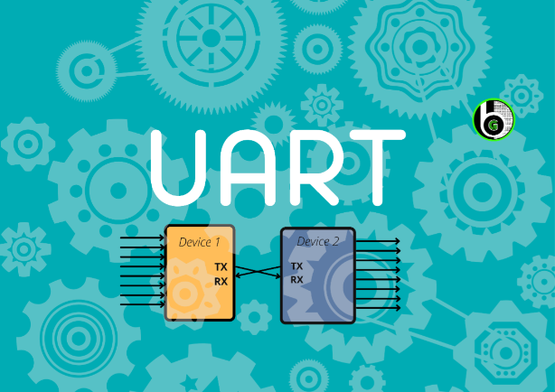
UART stands for Universal Asynchronous Receiver/Transmitter. As we can understand by the name it says it receives and transmits asynchronously. Asynchronously means it doesn\’t use clock pulse to synchronize the transmitter and the receiver.
In UART, the transmitter takes the signals in parallel from a controlling device[ex-CPU] then it sends the bits to a receiver in serial then the receiver converts those bits in parallel again. UART follows one master one slave approach as it uses only 2 wires for communication. It has one transmitter and one receiver.
How does it work?
As I, ve mentioned above it transmits asynchronously hence it uses a start and stops a bit, in it contains main data and a parity bit. The parity bit is only needed if the device needs to check the error.
When the device wants to start the communication, it pulls the transmitting line low which means it sends a 0 bit and receiving device understands that the transmitter wants to send the data. When the transmission line goes lows it stays low for one clock pulse and then it starts sending the data of 8 bits then the 9th one is a parity bit, the last one is stopping bit it stays high for the one clock pulse until the transmitter sends a low bit to start another frame.
To get, in detail understanding on UART Protocol, refer to this blog.
SPI Protocol
What SPI Protocol is?
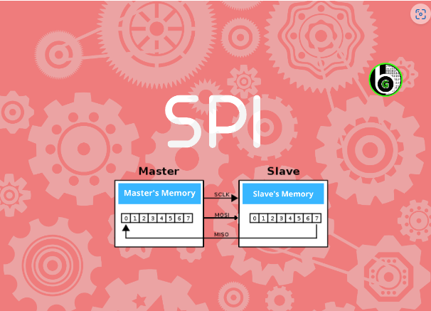
SPI stands for Serial Peripheral Interface. Just like UART it also uses Serial Communication for transmitting and receiving data but instead of asynchronous it uses synchronous communication protocol for transmission.
Synchronous means the transmitter and the receiver must have the same clock signal. It uses a Full duplex communication protocol which means it can send and receive at the same time. SPI follows one Master multiple slave configuration.
This protocol has 4 parts
1. MOSI-Master Out Slave In
Here Master sends data to the slave and the slave receives the data. Master sends data to each device it is connected to via a single wire.
2. MISO-Master In slave out
Here Slave sends the data to the master and the master receives the Data. Master receives the data from each device it is connected to through a single wire.
3. CLK-Clock Signal
It is important for synchronizing the data when the master sends or receives it.
4. CS/SS-Chip select/slave select
We have different wires connected to the chips. Suppose we have 3 chips connected. Then the master would have three wires cs1,cs2,cs3 connected from chip1, chip2,chip3 individually.
To get in detail understanding on SPI Protocol, refer this blog.
I2C Protocol
I2C stands for the inter-integrated circuit. If you have read carefully about SPI and UART you will find I2C got the best features of these two.
It follows multi-master protocol as multiple masters through a single slave or to multiple slaves. It is a half-duplex communication protocol since it has only one line for transferring and receiving data. It is also called Two Wired Interface as it uses two wires for communication.
This protocol has 2 parts
- SDA: For sending bits
- SCL: For synchronizing the data.
How does it work?
In I2C as we have multiple slaves, every slave must have a different address before sending a bit master will address or call the receiver. If we have multiple masters then the master will check the clock signal. If it is high it will send the data or if it is low then it means another master is sending the data at the moment.
To get more in detail understanding of I2C protocol, refer to this blog.
Conclusion Para
- In the end, if you want to use two devices then UART works best and fastest.
- If you have multiple slaves and one master then I would suggest going for SPI
- And if you want to connect one slave with multiple masters then I2C is the fastest as it lowers the wirings as well.
Other blogs to explore
About Microcontrollers
About IoT
BootLoader EXPLAINED!
What is BootLoader(BL)? The bootloader is a small chunk of code that gets executed when the MCU powers on or resets. Its main function is to manage the initial startup process, including any necessary checks or updates before the main application code runs. How BootLoader(BL) is different from Application Software? Application Software is the function-specific code that you program to perform an MCU-based task(like controlling the motor, displaying information, etc,). But you must be thinking or saying, that your application software also behaves pretty same as bootloader cause everytime you start/reset MCU, it will restart your application code from the beginning, right? But there’s a quite crisp gap between this BootLoader and Application Software which can broaden your understanding of bootloader and application software. Let’s divide this crisp gap into 3 sub-domains: Memory Allocation: If I talk about memory occupied by BL and Application Software. The first thing would be where are these two located and in which memory, answering that, BL is located at the beginning of FLASH memory and it always has some reserved space only which is also write-protected(Thinking why write-protected because to prevent accidental overwriting during normal operation) whereas application software is also stored in FLASH memory only but it’s below the space allocated to BL. Execution Flow: Upon power-on or reset, the microcontroller’s program counter starts executing code from the beginning of the flash memory, where the bootloader is located. After the bootloader completes its tasks (like, checking for updates, and validating the application), it will typically jump to the application’s start address (which is known and fixed in the bootloader code) to begin executing the application. Update Process: A well-developed bootloader can help you even in handling firmware updates. It can receive new application code, erase the old code, and write the new code to memory. The application cannot typically update itself. It relies on the bootloader to manage this process. The application’s major focus is on running the device’s features and does not deal with the update or integrity checks. Let’s understand with a analogy Taking an analogy with our expertise field of automotive embedded systems. Considering ourselves as an OEM, we have been reported a problem. A software bug is discovered in the ECU that controls the braking system. This bug causes the braking system to occasionally misbehave under specific conditions, such as when the vehicle is driving downhill. Diagnosing this issue requires an early solution because the bug needs to be fixed quickly to ensure the safety of the vehicles on the road. During the update of this bug fixing, the vehicle’s battery drains, and the update process is interrupted: With a Bootloader: When power is restored, the bootloader detects that the application firmware is corrupted or incomplete. It can either retry the update automatically or revert to a backup firmware version, ensuring the vehicle remains operational and can be updated again. I agree in this condition driving is not safe, but at least the car can operate so that it can be driven to repair with full caution. Without a Bootloader: The ECU might attempt to boot the corrupted application, resulting in a system crash or malfunction. The vehicle may not start or may exhibit erratic behavior, requiring a technician to manually intervene and repair the ECU, which could be time-consuming and costly. EDIT: Just found another real-life example. As we all know windows push too much of FOTA(Firmware Over-The-Air), out of which some take too much time to restart and some get applied with restart. Now you must have seen this screen will update. This “DON’T TURN OFF YOUR COMPUTER” message is also displayed for the very same reason, how power disruption can lead to the bricking of your laptop. But you must be curious what exactly what will happen if I cut off the power supply, and power up the device again, right? As a bootloader function, this interruption will be acknowledged and the bootloader will roll back to the previous functional update. You might see below mention image on start-up. IMPORTANT: Avoid trying this at home, this maneuver costs us to retrieve the data but unfortunately all core OS files and applications were corrupted and no longer responded for usage, we tried some troubleshooting using the window troubleshooter, but it wasn’t effective. At last, we installed a completely fresh OS from scratch. I would expect that you have completely understand the “WHY” and “WHAT” of BootLoader. Now, it’s time to understand the “HOW” of bootloader. Important Terminology in BootLoader Memory Management Memory management is quite an interesting concept that can also help in relating to real-world applications. As we understand the chronology of the working of a bootloader, which is firstly a bootloader will get which now will be followed by application software. Now basically there can be different executions of application software, let’s brief all possible ways: Executing Directly from Flash Memory: This specific condition is noticed in most of the embedded MCUs where the bootloader and application software are placed in FLASH memory only. Flash memory is non-volatile, meaning it retains data even when the power is off. Copying to RAM Before Execution: In some cases, the application code might be copied from flash memory to RAM before execution. This approach is more common in systems where high performance is required or where the flash memory is slower than RAM. The major reason behind using RAM for execution, RAM is typically faster than flash memory. Overlaying: In systems with limited RAM, overlaying is a technique where only a portion of the program is loaded into RAM at any given time, with different parts of the program being loaded and unloaded as needed. Virtual Memory Techniques: This specific technique is very common nowadays you must see that recent smartphones have this feature called RAM EXTENSION, where a portion of storage is accumulated to RAM for its R/W access. Parts of the application can be swapped in and out of physical RAM as needed. Such strategies
GPIO Peripheral in S32K144 MCU
What is GPIO peripheral in NXP S32K1xx MCU || Briefing about how to use GPIO peripheral in NXP S32K1xx MCU’s
UART Peripheral in Microcontroller
Explore this blog to know about UART peripheral in Microcontroller for doing UART communication
Starting Up with AVR
Table of Contents Introduction AVR stands for a Alf and Vegard’s RISC processor and is a microcontroller. Microcontroller is like a mini computer or a processor dedicated for a particular task. We can code AVR using C, C++ or Assembly language. AVR PINOUT Brief description of AVR pins Pin 1 – Pin 8 (PB0 – PB7): General Input / Output pins used as GPIOs i.e. General purpose Input-Output. Pin 9: It is a reset pin and resets the microcontroller. The bar above the RESET represents that it is active low i.e. when the reset pin is grounded then it resets the microcontroller. Pin 10, Pin 11 (Power Supply): These pins are used to give power to the microcontroller. We give a positive line to the VCC (Pin 10) and ground to GND (Pin 11). Generally, 5V is given as input. Pin 12, Pin 13 (Crystal Oscillator) : These pins are used to connect a crystal oscillator with AVR to give it an external clock. Pin 14 – Pin 21 (PD0 – PD7) : General Input / Output pins used as GPIOs i.e General purpose Input Output. Pin 22 – Pin 29 (PC0 – PC7) : General Input / Output pins used as GPIOs i.e General purpose Input Output. Pin 30 (AVCC) : It is used to provide power to Analog to Digital Converter of AVR. Also provides immunity to noise while conversion. Pin 31 (GND) : It is a common ground provided to be used. Pin 32 (AREF) : It is used to give a reference voltage to Analog to digital converter of AVR. Pin 33 – Pin 40 (PA0 – PA7) : These pins are used to take analog input and have Analog to Digital converter. For eg: we can sense temperature and convert from values 0-255 (8 bit) or 10 bit values. Programming AVR For any microcontroller to perform any action we need to put some code i.e. a set of instructions in it which it can follow. We write code in computer and then transfer the code to microcontroller using specific toolchain. For AVR MCU, we can write code using different IDE like Atmel Studio, Arduino IDE, VsCode in Embedded-C language, C and C++ for hardware purposes. Some SDK used for writing code of AVR are ATMEL STUDIO IDE, Arduino IDE, WinAVR etc. All of the mention SDK are recommended where Atmel Studio is a bit heavy software with loads of features for high performance laptops whereas WinAVR is a really light software to achieve the main motive of AVR coding with some basic and few extra features. WinAVR is recommended for people with laptops having low configurations. WinAVR is a pretty simple tool and can be installed easily. Here we will be discussing on how to install and get Atmel Studio ready for coding of AVR. Setting Up Atmel Studio You should refer to Video 6 – Video 9 of the following playlist created by Gettobyte for detailed tutorial on Atmel Studio. AVRDude AVRDude is a tool or so called utility to download/upload/manipulate the contents of ROM and EEPROM of AVR microcontrollers using your PC and uses ISP i.e. in system programming technique. It is a command line tool and has a huge list of commands which can be referred from its documentation or directly found from the internet as required. Link of Documentation is provided : http://download-mirror.savannah.gnu.org/releases/avrdude/avrdude-doc-6.3.pdf. For quick reference you can also use command: ‘avrdude help’ in command line. To use avrdude, you need to first download and install it which can be done from the provided link: http://download.savannah.gnu.org/releases/avrdude/avrdude-6.3-mingw32.zip. After downloading follow the below steps: 1) Copy the address of folder containing unzipped files 2) Type Env in search bar in start 3) Select ‘Edit the system environment variables’ 4) A dialog box will pop up. Click on environment variables in bottom right corner. 5) Select ‘Path’ in ‘System Variables’. 6) Click on edit button below system variables box. 7) Click on ‘New’ 8) Paste the address that you copied. 9) Click ‘Ok’ on all the dialog boxes. Now you are AVRDude is setup and ready to use. Applications and use of AVR AVR consist of multiple input output pins, ADC, oscillator, timer, interrupts and many more features hence useful in integrating multiple sensors and actuators (Devices that takes signal from microcontroller to perform some action in real world). This lead to use of AVR in variety of applications like home automation, automobiles, medical devices etc. AVR comes in small size with less memory as well as big size with huge memory size and more processing power and features to cover from most simple to much complex applications. Conclusion Congratulations, now your pc is completely ready to code AVR microcontroller. In further blog series of AVR we will dive deep into concepts of programming the AVR and understand different concepts of AVR programming, AVR microcontroller and electronics itself so stay tuned!! Author: Kunal Gupta
CAN Bit Timing Explained
Discover how CAN bit timings are calculated for CAN Nodes while using CAN Technology. Knowledge of synchronization between ECU’s while doing Controller Area Network Communication.
Debugging Technology in Microcontrollers
Want to know how to debug the microcontrollers? Want to know how to use debugging tools like step-in, step-out, breakpoints and etc. If yes then you have to right place. Explore this blog to understand about Debugging technology in microcontroller’s with NXP S32K144 MCU using ElecronicsV2 board
Author: Kunal Gupta
Author