
Serial communication
In serial communication, we have only one line for transmitting and receiving data which is why it is half-duplex. It is best for high frequencies as it uses only a single bus or channel for communication, but it can be a bit slower than parallel as it sends only a single bit per clock pulse also because of the single wire here we have fewer chances of cross-talks. It can detect the error as well.
When transferring a bit quick change in voltage are required like for 5v OS, 0 bit communicated as a short pulse is 0v, and 1 bit communicated by a short pulse of 5v. In serial communication, the first bit is the most significant bit and the last one is the least significant bit.
Parallel Communication
In parallel communication, we have a number of lines or buses equal to the number of bits we are transferring. We call it full duplex as the line for transmitting and receiving bits is different. It is faster for small frequencies as all bits are sent at once but as we have to use multiple wires it is costlier also here, we have lots of chances of cross-talks.

As in serial, here also we have the first bit is the most significant bit and the last one is the least significant bit.
UART Protocol
What is UART Protocol?
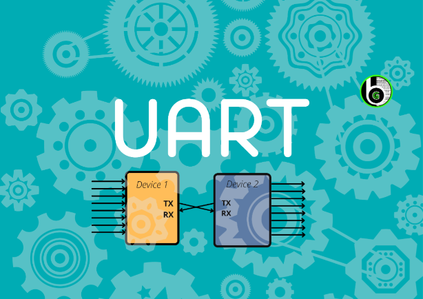
UART stands for Universal Asynchronous Receiver/Transmitter. As we can understand by the name it says it receives and transmits asynchronously. Asynchronously means it doesn\’t use clock pulse to synchronize the transmitter and the receiver.
In UART, the transmitter takes the signals in parallel from a controlling device[ex-CPU] then it sends the bits to a receiver in serial then the receiver converts those bits in parallel again. UART follows one master one slave approach as it uses only 2 wires for communication. It has one transmitter and one receiver.
How does it work?
As I, ve mentioned above it transmits asynchronously hence it uses a start and stops a bit, in it contains main data and a parity bit. The parity bit is only needed if the device needs to check the error.
When the device wants to start the communication, it pulls the transmitting line low which means it sends a 0 bit and receiving device understands that the transmitter wants to send the data. When the transmission line goes lows it stays low for one clock pulse and then it starts sending the data of 8 bits then the 9th one is a parity bit, the last one is stopping bit it stays high for the one clock pulse until the transmitter sends a low bit to start another frame.
To get, in detail understanding on UART Protocol, refer to this blog.
SPI Protocol
What SPI Protocol is?
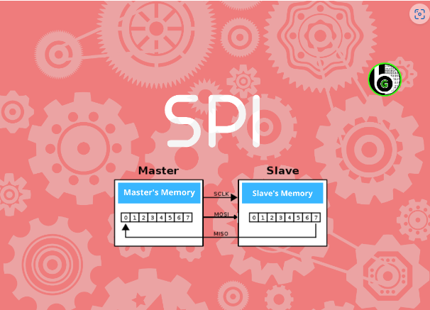
SPI stands for Serial Peripheral Interface. Just like UART it also uses Serial Communication for transmitting and receiving data but instead of asynchronous it uses synchronous communication protocol for transmission.
Synchronous means the transmitter and the receiver must have the same clock signal. It uses a Full duplex communication protocol which means it can send and receive at the same time. SPI follows one Master multiple slave configuration.
This protocol has 4 parts
1. MOSI-Master Out Slave In
Here Master sends data to the slave and the slave receives the data. Master sends data to each device it is connected to via a single wire.
2. MISO-Master In slave out
Here Slave sends the data to the master and the master receives the Data. Master receives the data from each device it is connected to through a single wire.
3. CLK-Clock Signal
It is important for synchronizing the data when the master sends or receives it.
4. CS/SS-Chip select/slave select
We have different wires connected to the chips. Suppose we have 3 chips connected. Then the master would have three wires cs1,cs2,cs3 connected from chip1, chip2,chip3 individually.
To get in detail understanding on SPI Protocol, refer this blog.
I2C Protocol
I2C stands for the inter-integrated circuit. If you have read carefully about SPI and UART you will find I2C got the best features of these two.
It follows multi-master protocol as multiple masters through a single slave or to multiple slaves. It is a half-duplex communication protocol since it has only one line for transferring and receiving data. It is also called Two Wired Interface as it uses two wires for communication.
This protocol has 2 parts
- SDA: For sending bits
- SCL: For synchronizing the data.
How does it work?
In I2C as we have multiple slaves, every slave must have a different address before sending a bit master will address or call the receiver. If we have multiple masters then the master will check the clock signal. If it is high it will send the data or if it is low then it means another master is sending the data at the moment.
To get more in detail understanding of I2C protocol, refer to this blog.


How Cryptography in Automotive is implemented.
In the new age of autonomous and connected vehicles, cyber-attacks in automotive are happening frequently. Discover in this blog, what technology is used to make our vehicles safe and secure.
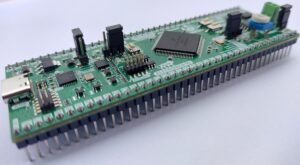
ElecronicsV3 Automotive Board (SHE Crypto Peripheral + CAN)
Low cost Development Board for NXP S32K144 MCU as beginner friendly automotive kits
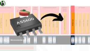
AS5600 Rotary Encoder Sensor Driver Stack with Autosar I2C Layer
GET IN TOUCH Contact us Got something on your mind? We’re all ears! Whether you have burning questions, awesome ideas,
Potentiometer Interfacing with S32K144(Elecroncics V3)
Interfacing10KOhm Potentiometer using ADC Driver of Autosar MCAL Layer via ElecronicsV3 Board (S32K144 MCU)
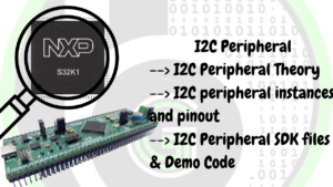
I2C Peripheral in S32K144
I2C Peripheral in S32K1 Microcontroller. How to use I2C peripheral of S32K1 Microcontrollers

A Deeper Dive into the fields of Artificial Intelligence
So far, we’ve learned about the types of AI, Family of AI, its features and limitations. Here, in this blog,