


AutoCal Course-v1
Excited with the automotive technologies?? Want to learn the software technologies, which runs the vehicles around us!!! And not just
Free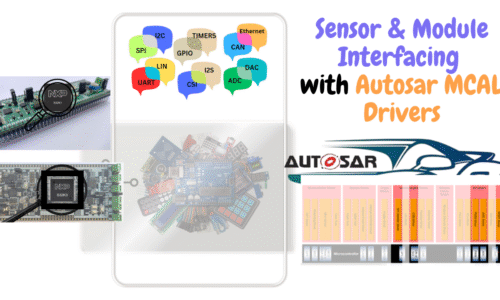
Automotive Sensor and Module Interfacing(ADAS)
Automotive Sensor and Module Interfacing(ADAS)
₹20,000.00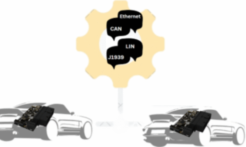
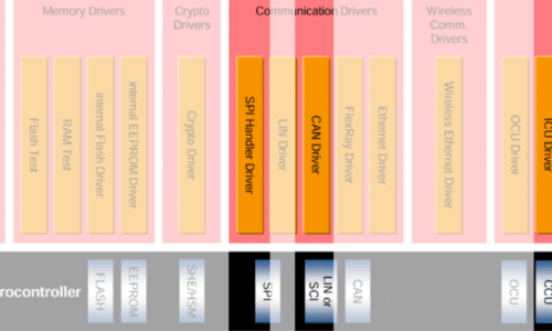
AutoProtocol Course-V1
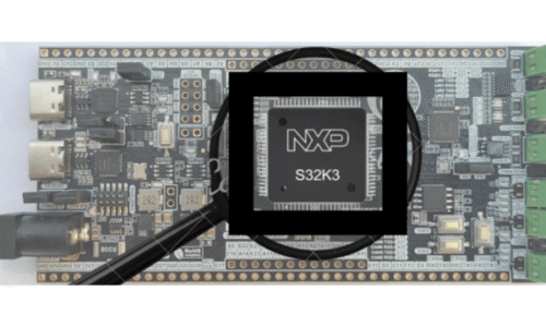
Learn Different Automotive protocols like: CAN, LIN, Ethernet, using Autosar MCAL Drivers and ElecronicsV3(S32K144 MCU)/AutoBoardV1(S32K344 MCU)
Free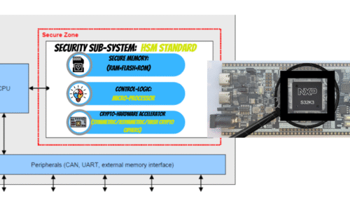
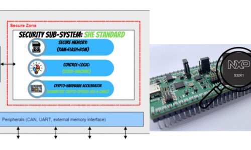
Cryto Security Model: Hardware Security Peripheral’s (HSM) using S32K3xx
Cryto Security Model: Hardware Security Peripheral’s (HSM) using S32K3xx
₹10,000.00


- All Posts
- Blog

The basic premise of search engine reputation management is to use the following three strategies to accomplish the goal of...
The basic premise of search engine reputation management is to use the following three strategies to accomplish the goal of...
The basic premise of search engine reputation management is to use the following three strategies to accomplish the goal of...
The basic premise of search engine reputation management is to use the following three strategies to accomplish the goal of...
The basic premise of search engine reputation management is to use the following three strategies to accomplish the goal of...
The basic premise of search engine reputation management is to use the following three strategies to accomplish the goal of...
The basic premise of search engine reputation management is to use the following three strategies to accomplish the goal of...

The powertrain domain includes key components such as the engine, transmission, and energy management systems, responsible for vehicle propulsion. With the rise of EVs and hybrid vehicles, real-time optimization through Edge AI is crucial, while Cryptography ensures protection against malicious data manipulation.

The chassis domain governs vehicle stability, suspension, and braking systems, ensuring safe handling and ride comfort. Edge AI enhances adaptive performance, while Cryptography prevents cyber threats from interfering with safety-critical functions

The body control domain handles vehicle access, lighting, climate control, and in-cabin automation. Edge AI enables intelligent automation, while Cryptography ensures only authorized commands are executed.
HMI systems enable driver interaction through touchscreens, voice commands, and gestures. Edge AI personalizes the user experience, while Cryptography protects against unauthorized access and data breaches.

The telematics domain includes GPS tracking, vehicle connectivity, and over-the-air (OTA) updates, essential for modern automotive ecosystems. Edge AI enhances predictive analytics, while Cryptography safeguards data integrity.

This domain includes Advanced Driver Assistance Systems (ADAS), collision prevention, and occupant protection technologies. Edge AI enables real-time risk assessment, while Cryptography ensures sensor data authenticity.