
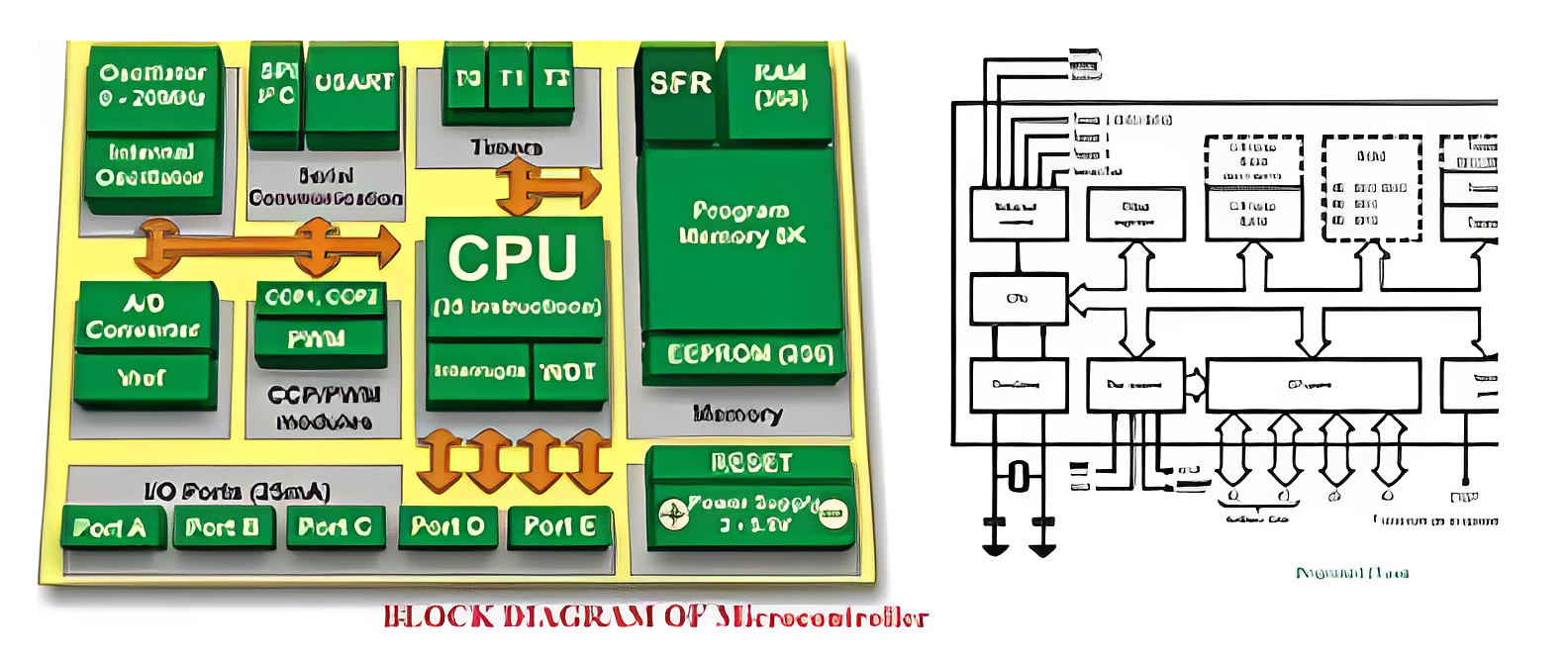


GPIO Peripheral in STM32F103 MCU
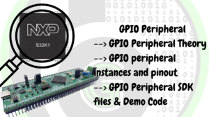
Table of Contents GPIO Theory So now we’ll talk about GPIO pins . GPIO stands for general purpose input output
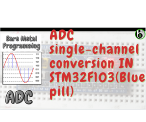
STM32F103 & ADC: Single Channel Conversion
In the last post, we have gotten to know about the features of ADC Peripheral that we have in STM32
PWM on STM32F103
What is PWM? PWM or Pulse Width Modulation, is a type of digital electrical signal which is periodic in nature,
Light Beige Sleek and Simple Blogger Personal Website by KsmaVideoEditor harsh gettobyte technp;pgies
Getting Hands-On with NXP eIQ: A “No Code” Starter Guide for Edge AI Developers
Introduction In a world driven by AI and IoT, deploying machine learning at the edge has become essential. NXP’s eIQ™
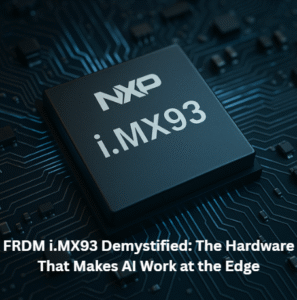
FRDM i.MX93 Demystified: The Hardware That Makes AI Work at the Edge
Imagine you’re handed a powerful little board, no bigger than your palm. At first glance, it looks like a jungle
How to Run AI on a Microcontroller or Microprocessor – A Beginner’s Guide to Edge AI
In the last few years, Edge AI has rapidly transformed how devices understand and interact with the world — without
Edge AI ToolKit: EiQ AI SDK
Introduction to EiQ In previous blogs, we’ve discussed in depth Edge AI, its features, advantages, and future scopes. Implementation of