
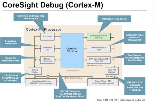

Now, in this Blog we will implement the theoretical knowledge of previous blogs to action and do them practically! We will do so by exploring the Trace Features in STM32MCU practically (STM32F103 Blue pill) using STLINKv2-B ( Official one white one) in STM32CubeIDE. 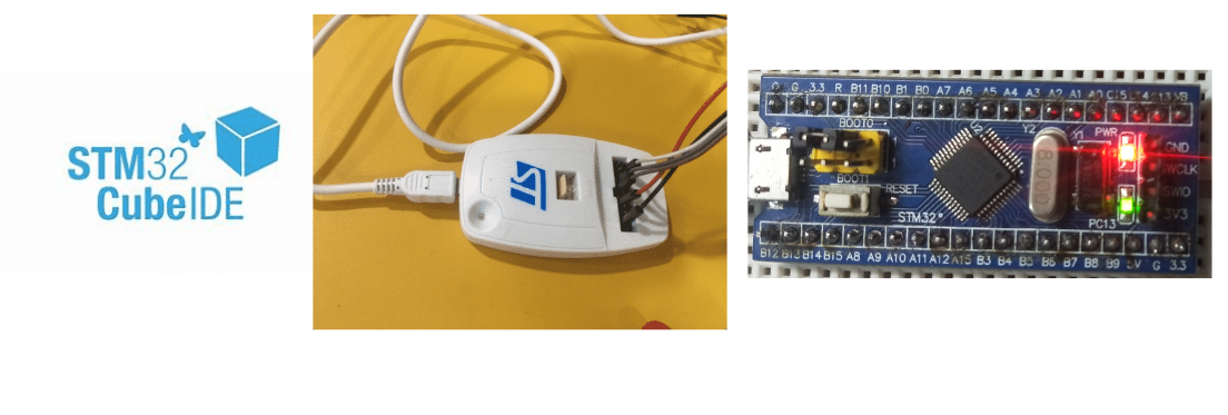

The STLINKv2 Programmer comes in with following things as u open its Box.
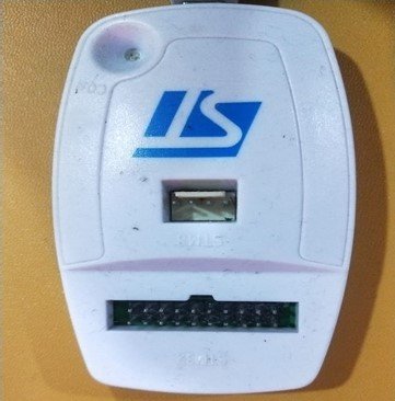
- Main STLINKv2 Programmer and Debugger
- 20 Pin JTAG connector
- USB 2.0 A to USB 2.0 Mini B
- 2 x Connecting Cable for STM8 SWIM
Now coming to the pain Connections for connecting STM32 MCU with STLINKv2.
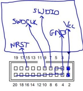
Programmer has the following pins for connecting it to STM32 MCU(Blue Circle).
These Pins have Pinout like these:
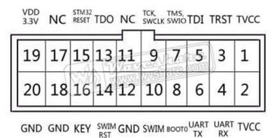
Right side from the Embarked Area (Orange Color), is pin 1 of the Programmer and then the pinout goes as shown in above pic.
Now the Essential Pins out of these 20 pins of the STLINKv2 programmer to Program and Debug STM32 MCU using ARM Proprietary SWD Protocol are only 5 pins.
- SWIO/TMS(Pin 7) à SWD PIN
- SWCLK/TCK(Pin 9) à SWD PIN
- TDO/SWO(Pin 13) à SWO PIN
- STM32 RESET(Pin 15) à RESET PIN
- VCC(Pin1&2) à POWER PIN
- GND(Below Horizontal line’s any pin can be used as GND except 2) à POWER PIN
SWD Pins of STM32 MCU will be connected to SWD PIN if we want to only use Debugging features alongside Programming the Microcontroller. Like as shown in PIC. 
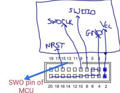
Now for Using the Trace Features we must connect one additional Pin from the Programmer to OUR Microcontroller and that is SWO Pin (13th pin) of Programmer to the Respective Trace SWO Pin Of our STM32 Microcontroller.
In STM32F103 SWO PIN is PB3 as shown in this schematic.
So, for Using Trace Features Connections will be like this.
To be noted down:
- Any pin from the below horizontal line except the VCC pin of that line can be taken as GND pin when using SWD/SWD+SWO pins and can be connected to GND pin of our STM32 MCU.
- Sometimes or in some Programmers we have to short all the VCC pins by Jumper wire for Proper connections or encase device isn’t able to power up MCU or Program it.
- In some cases, VCC pins 1&2 can be wrongly mapped in Some Programmer, and they can be at left hand side of the programmer that is at pins 19 and 20. So in case MCU does not Power up by above connections, then do not panic just change the VCC Pins and it might work out. ( This is in my case, so below pitcher is according to that)
Now so after successful Connections between STLINKv2 and STM32 MCU, Connect the USB cable between STLINKv2 and Laptop and LED light on the programmer will lighten up in RED color.
Figure 5 (These are the Final Connections For SWD+SWO)
Now I will be Showing STM32CubeProgrammer and STM32Cube IDE In this blog in software part.
First with STM32CubeProgarmmer:
As u connect your STLINKv2 Programmer to your computer, IN STM32CubeProgrammer u will see the Serial Number of Programmer if all goes well. As shown in Pic.
Figure 6
Now as u click on Connect Button by selecting STLINK, u will see all the details of Your respective MCU details and showing its memory Content. (In doing so Your programmer will start blinking in red, green color and Screen of STM32CubeProgrammer might take 1-2 secs of time for showing Memory contents and MCU details.)
Figure 7
This is just Demonstration of Successful connections of STLINKv2 and MCU for SWO+SWO pins and established Communication between Programmer and Laptop via STM32Cube Programmer.
As if now, we have not used the trace features, for using that we must create a project and Upload in MCU by things mentioned in below section.
For STM32CubeIDE also follow the below section
If any Error comes in while connecting the STLINKV2 , FOLLOW this video for solving all kinds of Errors and to get Solutions for them.
Create a New Project in STM32CubeIDE by choosing your corresponding Workspace (Figure 1), select Your MCU in Board Configuration Window (Figure2) by selecting the MCU you are using.
Figure 8

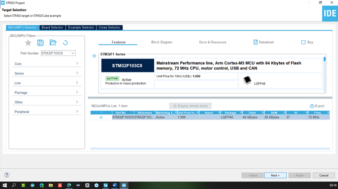
Figure 9
Now name Your Project in next window and choose the targeted language according to your choice and Select Executable in Targeted Binary Type.
In Target Project type their will be 2 Options,
STM32Cube and Empty.
(In this Blog I will be telling things according to STM32cube project type. By selecting STM32Cube, Auto generated code STM 32 HAL initializes all the Processor registers for using Debug and Trace features according to the configurations made in STM32CubeMX window.)
Now in Cube MX configuration window we must Select RCC Mode for HSE as Crystal/Ceramic Resonator and Debug Mode as Serial Wire,
Under Pinout and Configuration window select the System Core and in it Select the RCC and SYS. Select the corresponding Options as shown in pics below.
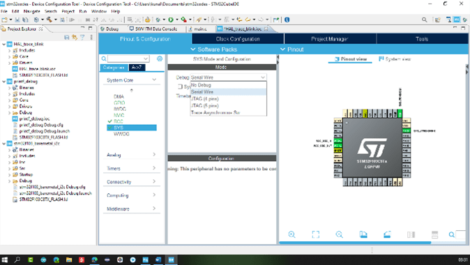
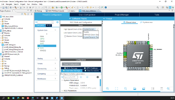
Figure 10
And then in the clock Configuration window Select the Clock Frequency according to your choice. I am selecting 32Mhz in my case for STM32F103 using HSE (which has input frequency of 8 MHz and selecting PLL as clock Source for System clock).
I am configuring the Onboard LED on STM32F103 Blue Pill as GPIO OUTPUT just for demonstration purpose. That is pin PC13.
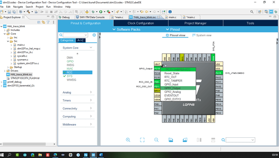
Figure 11
And then save the file and Autogenerated code Process using STM32HAL will be started.

Figure 12
Now open the main.c file of Your project from the Project explorer window.
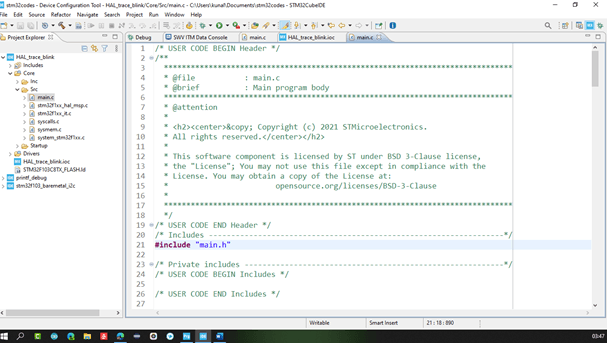
Figure 13
That is all for this Blog, second part of the Topic is in next Blog.
Follow the next Part for NEXT Part of the blog.
Playlist for Debugging techniques in Firmware development: https://www.youtube.com/playlist?list=PLb_Q-Ps0nJou2Ped93q02JRfiMCJorLYX

RECTIFIER CIRCUIT
Why do we need a rectifier Circuit? Whenever DC power is needed that time, we need to convert an AC
TIMER Peripheral in Microcontroller’s
Explore basics of TIMER Peripheral in Microcontroller!!
Introduction of Nordiac NRF5xx SoC\’s
Table of Contents Overview on Nordic IoT Chips Nordic Semiconductor is a semiconductor MNC, which designs & develops a wide
