Table of Contents
So hello guys, welcome back to NXP Semiconductors S32K144 MCU Tutorial series. In the last blog we just started with S32K144 MCU. In this blog we are going to explore the first peripheral of this MCU. Going to Start with GPIO peripheral. Objective would be to get
- familiarity with GPIO peripheral for S32K144 MCU.
- Would be understanding GPIO peripheral from Hardware point of view in S32K144 MCU.
- Going to understand the how to use GPIO peripheral via S32K SDK/pins driver.
- Would also be demonstrating the blink LED sketch for GPIO in the end.
So read along the blog and do tell me its reviews!
GPIO Peripheral Theory
General Purpose Input/Output(GPIO) is a crucial peripheral in microcontrollers, enabling interaction with the external world by sending and receiving digital signals.

Digital Signals, here are referenced as High and Low Signals. High signal is +5/+3.3V level and Low Signal is 0V level. As MCU’s are digital devices, so it can only understand High and Low Voltage levels.

Almost all the pins of the Microcontroller are by default part of the GPIO peripheral, accept from the power pins. Every Pin can be configured in Input or Output State.
State of Pins

- When a pin is configured as Input State, it can detect the level of external signal whether it is high signal or low signal. For example when we press the button, MCU process that as a external signal.
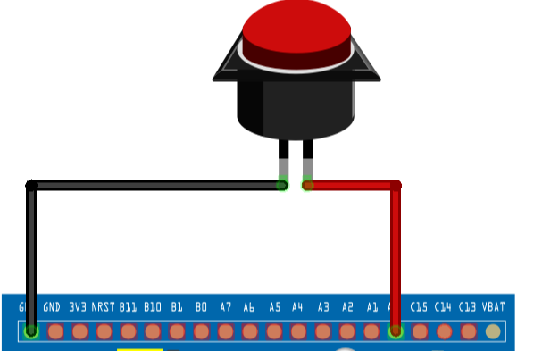
GPIO as Input signal
Button is connected to one of the GPIO pins of the Microcontroller, which is being configured as Input state and when we press the button a High or Low voltage signal is generated. Which voltage level is generated? is detected by the configured GPIO Pin.
- When a pin is configured as Output State, it can generate the High Signal or Low Signal to drive the external electronic devices. For example, LEDs are electronic devices which needs High signal to power-on them and low signal to power-off them.
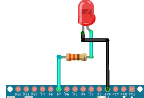
GPIO as Output signal
So LEDs are connected to one of the GPIO pins of the Microcontroller, which is being configured as Output State and then by programming we can configure the signal that has to be generated from the corresponding configured GPIO pin.
Input/output are defacto states of pins, apart from these 2 there are other states too, on which pins can be configured.
State of pins can be:
- Output
- Input
- PullUp
- PullDown
- Tri-state
GPIO pins categorization
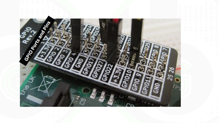
GPIOs are organized into banks, each requiring a unique identifier to identify a specific pin. These identifiers are commonly referred to as “Ports” and “Pads”. With the vast number of pins available on a microcontroller, it is essential to have a mechanism to reference and utilize them effectively.
To simplify this process, GPIO pins are now divided into Ports, with each Port containing a multiple of 8 pins. This division allows for easy referencing and addressing of the pins on the microcontroller.
By utilizing this system, developers can efficiently access and manipulate the GPIO pins on a microcontroller, streamlining the development process and improving overall functionality.
GPIO In S32K144 MCU
In S32K144 MCU, there are 5 ports of GPIO: named as PTA to PTE. Each Port pin has 16 pins.
In S32K144 reference manual, GPIO peripheral is being dicided into 2 modules: PORT (Port Control and Interrupt Module) and GPIO (General Purpose Input/Output Module).
PORT Module is responsible for Interrupt and Port Control Operations (Like alternate functions, Pull-up/down, drive strength) of the above Ports specified. GPIO module is responsible only for Controlling Input/Output directions of the port pins.
Features of GPIO in S32K144 MCU
- Pins can be configured as Output.
- Pins can be configured as Input.
- Pins support the multiplexing of signals, so that a single pin can be do different job(refer to signal multiplexing section).
- Dedicated Port Output registers for set/clear/toggle the bits.
- Efficient bit manipulation of the general-purpose outputs is supported through the addition of set, clear, and toggle write-only registers for each port output data register.
- GPIO module can operate on 3 modes: Run Mode, Stop Mode and Debug Mode
- GPIO Module is clocked by System clock.
- GPIO module has a feature of Lock feature, in this feature we can lock the Mode of operation of PIN in one Power Cycle.
Registers of GPIO in S32K144
For simplicity, each GPIO port’s register appear with the same width of 32 bits, corresponding to 32 pins. The actual number of pins per port in S32K144 is 16 pins. So we will be addressing only first 16 bits of the registers, on last remaining 16 bits are irrelevant for us. But in S32K144 there are 16 pins only per port, so we will be accessing only first 16 bits of the registers (0-15), reading & writing on (16-31) will have no effect.
In S32K144, there are registers to support 8bit, 16-bit and 32-bit access. Registers of GPIO:
- GPIO Data Direction register: Direction of GPIO pin
- GPIO output data register: Output direction of GPIO pin
- GPIO Input Data Register: Displays the logic value on each pin
Efficient bit manipulation of the general-purpose outputs is supported through the addition of set, clear, and toggle write-only registers for each port output data register.
Each Port of GPIO has 16 pins. And each pin is referenced as each bit of the above registers.
Features of Pin configured as Output:
Output: Pin is configured for the GPIO Function and corresponding port data direction register bit is set.
For efficient bit manipulation, there are dedicated output registers for toggling, Set High or Set LOW the pins. Instead of doing the manipulation of pin signals via software using bit manipulation and shifting
Features of Pin Configured as Input
Input: If Pin is configured for the GPIO function and the corresponding port data direction register bit is clear.
GPIO Hardware/Pinout in S32K144 MCU
S32K144 MCU comes in 3 pin counts: S32K144_100lqfp, S32K144_64lqfp, S32K144_48lqfp. The one which we will be using is S32K144_100lqfp. S32K144 EVB board which is explained in last blog, has S32K144 MCU of S32K144_100lqfp packaging. 

For GPIO peripheral to use, in terms of Hardware first thing that is needed is pinout of the MCU.
To see the pinout of S32K144 MCU, you will not find that on its Datasheet or Reference Manual. But there is separate excel sheets to know details for its pinout, by the name of: S32K144_IO_Signal_Description_Input_Multiplexing.excel.
This excel is attached with S32K144 MCU reference manual. Open the Reference Manual of S32K144 with Adobe Acrobat and click on below highlighted icon. 
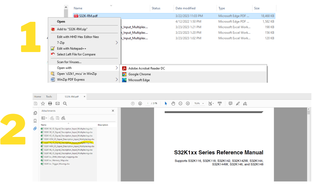
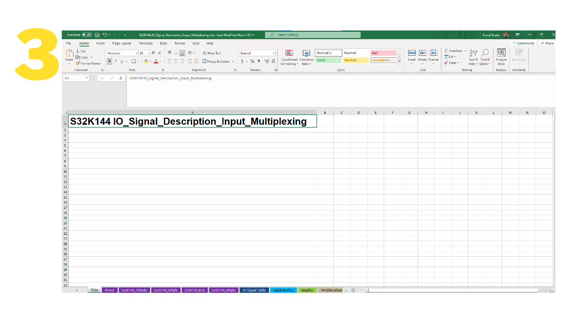
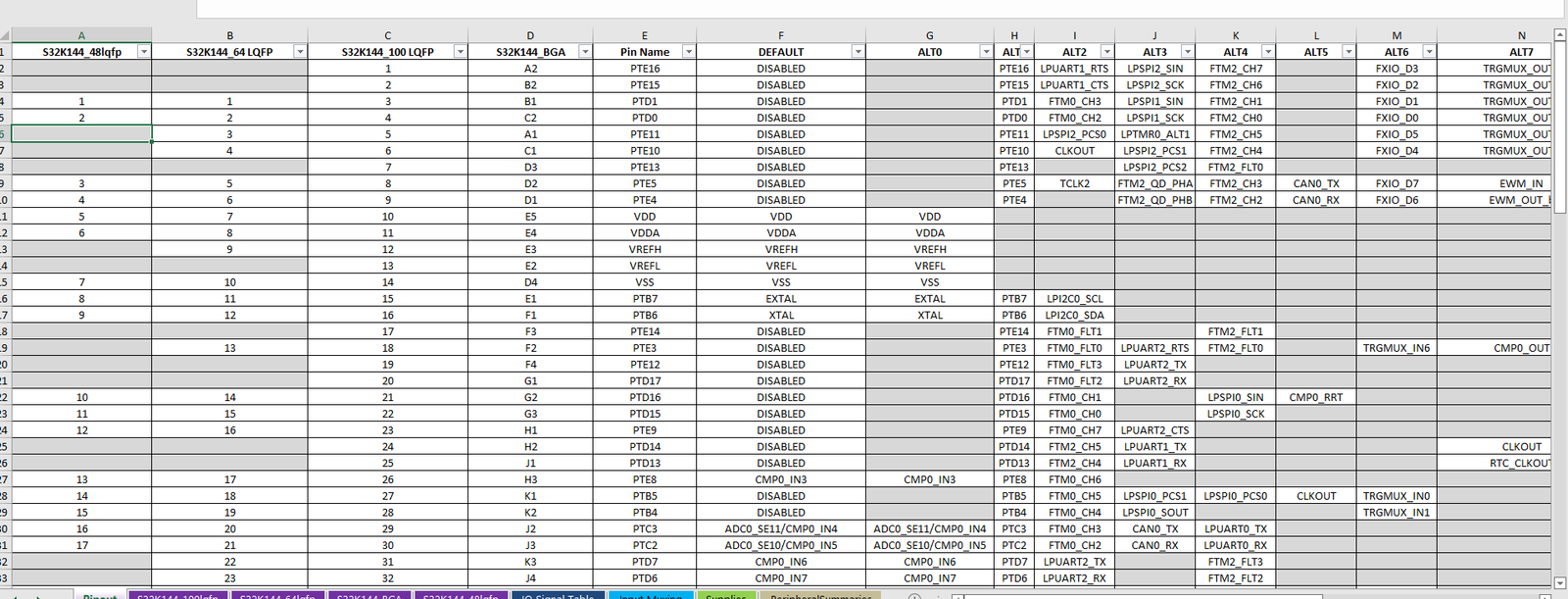
Now coming back to pinout of S32K144 MCU, this below is the pinout that is extracted from the excel sheet for the S32K144_100lqfp packaging. We would be referring this packaging only throughout the series,
One can see, that their are 100 pins in this MCU S32K144. Starting from pin 1 which belongs to PTE16 and pin 100 which belongs to PTA8.
As you can see there are so many, to use them we need to have some kind of referencing. Thus, concept of Ports is there. Their are total 5 Ports in S32K144 MCU and supply pins:
- PTA: PTA0-PTA17(18 pins)
- PTB: PTB0-PTB17(18 pins)
- PTC: PTC0-PTC17(18 pins)
- PTD: PTD0-PTD17(18 pins)
- PTE: PTE0-PTE16(17 pins)
- And 11 Supply pins (VDD, VDDA, VREFH, VREFL, VSS)
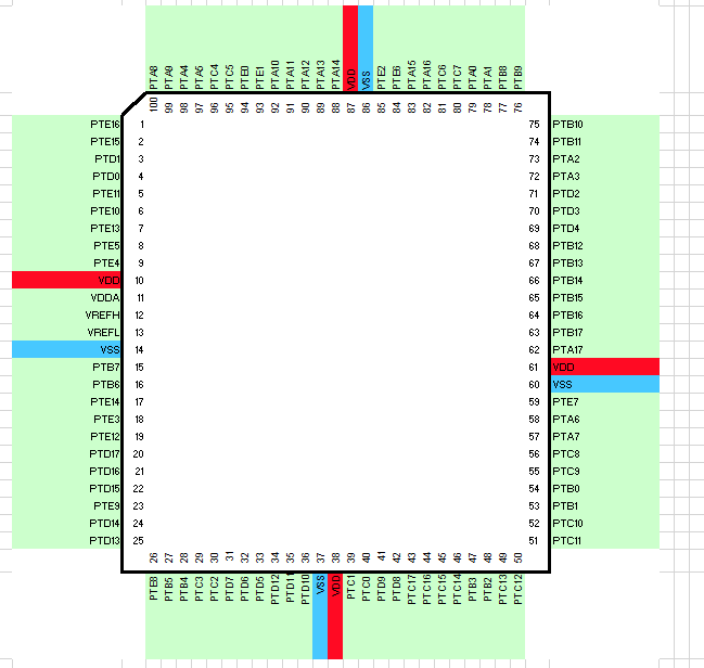
Now in the excel sheet one can find that there are multiple sheets as follows.
In this section, pins description according to MCU packaging and pin count size is listed.
Next 3 sections have the MCU pinout photo for the different packaging sections
In this section, in detail description for each Pin is there. Parameters like what all alternate functions that pin can have, its reset value, its direction, description and various other parameters are listed.
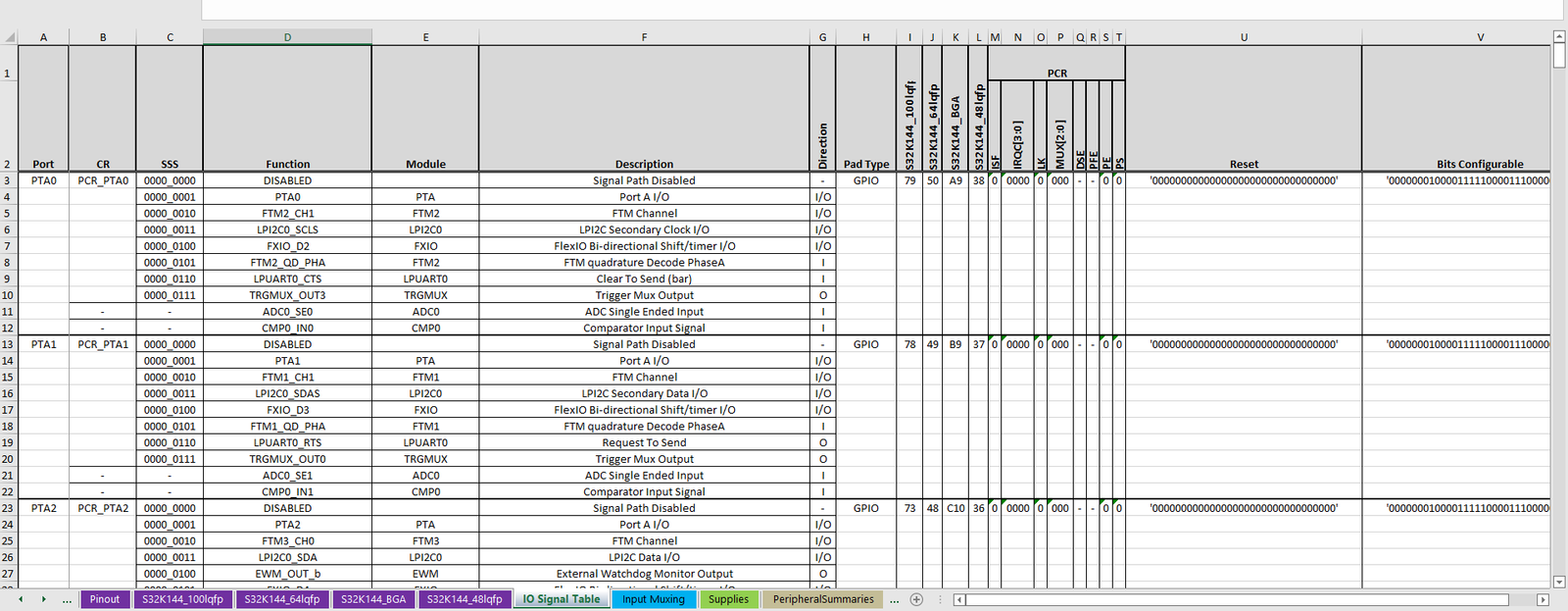
In this sheet, what all pins are there for specific peripheral pins. This sheet makes quite easy to figure which pin can be used for corresponding peripheral pins.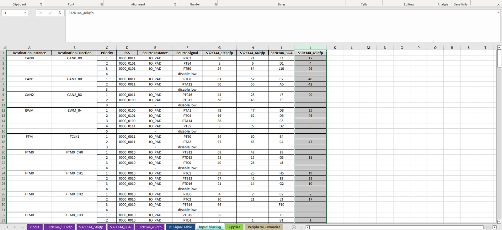
This sheet, has information about the supply pins of the MCU. Their are total 11 supply pins in S32K144 MCU.

This sheet summarizes what all pins are there are each peripheral.
Also in S32 Configuration Tool in S32 Design Studio one can see all the details of the MCU Pinout and description.( Will be telling more on S32 Configuration and S32 DS later.)
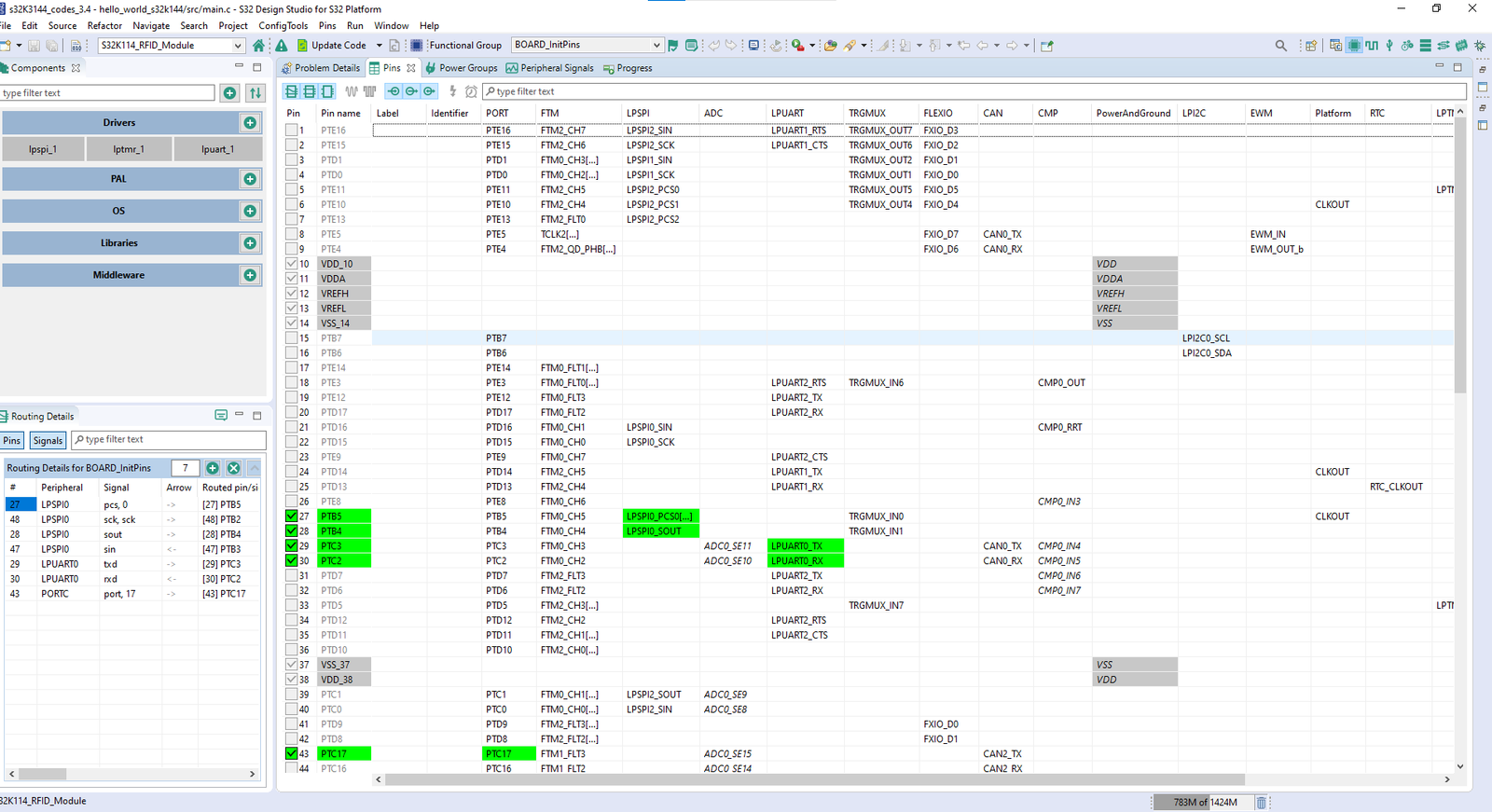
Now in S32K144 EVB Board, pin numbering is done in bit different way. Pin Naming is not done directly by the name of Pins name as referenced in Pinout Sheet. Instead, it is done in terms of Jacks. As shown in below pic.
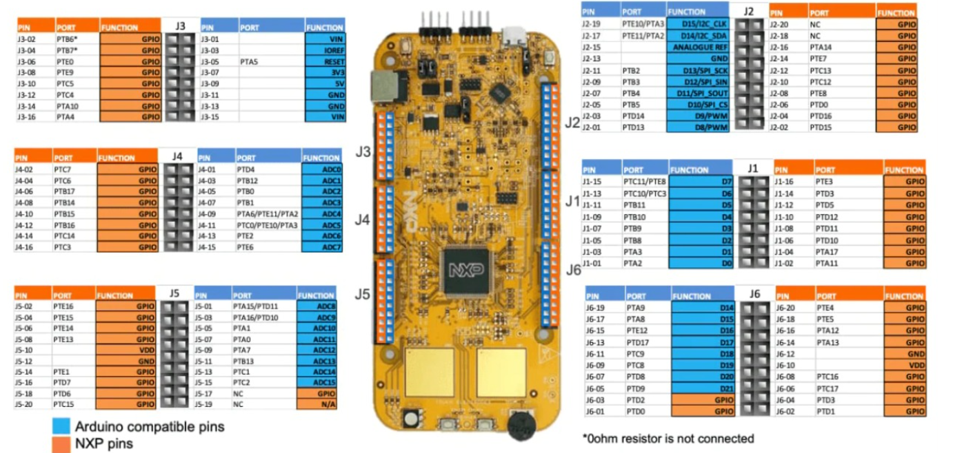
There are 6 Jack Connectors: J1-J6. All Jack are of Female Connectors(This might make the connections messy). J1 & J3 have 16 pin count. J5, J6 & J7 have 20 pin count. J4 have 15 There are. From the above pic you can refer out the Pin name of each Jack Pin. And then correspondingly get to know about that Pin via Sheet.
How to use the GPIO Peripheral in S32K144 MCU
So as to know about S32 configuration tool and how to configure/use the GPIO peripheral in S32K144 MCU, refer to this video.
GPIO SDK for S32K144 MCU
S32 SDK/ drivers provide an easy to use and quick way to use the GPIO peripheral in S32K144, which is known as Pin Driver. 
Each S32 SDK driver can be configured and enabled to use in the project via S32 Configuration Tool. Will be digging into that part, in next section. For now, let’s understand the Pin driver in more details, so as to use the GPIO periperal.
Broadly there are 5 files in Pin Driver, that controls the GPIO peripheral in S32K144 MCU:
- pins_driver.h
- pins_driver.c
- pins_gpio_hw_access.h
- pins_port_hw_access.h
- pins_port_hw_access.c
pins_driver.h & pins_driver.c are the GPIO Peripheral Abstraction Layer and Rest 3 are the GPIO low-level drivers of the GPIO peripherals.
GPIO Peripheral Abstraction layer functions are the ones that are directly used in main.c or Application code. And internally these functions use the GPIO low-level driver functions.
Thus, we would find that in Rest 3 files, most of the functions are static functions and static inline functions, as low-level driver functions are internally used in Peripheral Abstraction Layer functions. So that if hardware is changed, so only low-level driver functions would be changed. GPIO PAL functions would remain same and their would be very small amount of change required in Application code or main.c. This is how Code Portability and modularity is designed, providing efficient use.
Configuring GPIO Pins
First thing, that we need to do for using GPIO pins, is to configure them. By configure we mean:
- Which pin to use and that pin belongs to which port.
- pin to be used in what state or if pin to be used by other peripheral then configuring the state of pin according to that(pin multiplexing)
- to configure the features, like pullup/down resistors, slew rate, open drain, over current and etc( this is kind of chip specific, according to the chip their are different features)
To configure the GPIO pins, in pins_driver.h there is a structure pin_settings_config_t. This structure allows users to properly exploit S32K1 GPIO features.
/*!
 * @brief Defines the converter configuration
 *
 * This structure is used to configure the pins
 * Implements : pin_settings_config_t_Class
 */

typedef struct
{
#ifdef FEATURE_PINS_DRIVER_USING_PORT
    PORT_Type         *         base;              /*!< Port base pointer.                        */
#elif defined FEATURE_PINS_DRIVER_USING_SIUL2
    SIUL2_Type        *         base;              /*!< SIUL2 base pointer.                       */
#endif
    uint32_t                    pinPortIdx;        /*!< Port pin number.                          */
#if FEATURE_PINS_HAS_PULL_SELECTION
    port_pull_config_t          pullConfig;        /*!< Internal resistor pull feature selection. */
#endif
#if FEATURE_PINS_HAS_SLEW_RATE
    port_slew_rate_t            rateSelect;        /*!< Slew rate selection.                      */
#endif
#if FEATURE_PORT_HAS_PASSIVE_FILTER
    bool                        passiveFilter;     /*!< Passive filter configuration.             */
#endif
#if FEATURE_PINS_HAS_OPEN_DRAIN
    port_open_drain_t           openDrain;         /*!< Configures open drain.                    */
#endif
#if FEATURE_PINS_HAS_DRIVE_STRENGTH
    port_drive_strength_t       driveSelect;       /*!< @brief Configures the drive strength.     */
#endif
    port_mux_t                  mux;               /*!< @brief Pin (C55: Out) mux selection.      */
#if FEATURE_PORT_HAS_PIN_CONTROL_LOCK
    bool                        pinLock;           /*!< Lock pin control register or not.         */
#endif
#ifdef FEATURE_PINS_DRIVER_USING_PORT
    port_interrupt_config_t     intConfig;         /*!< Interrupt generation condition.           */
    bool                        clearIntFlag;      /*!< Clears the interrupt status flag.         */
    bool                        digitalFilter;     /*!< Enables digital filter.                   */
#if FEATURE_PINS_HAS_OVER_CURRENT
    bool                        clearOCurFlag;     /*!< Clears the Over-Current status flag.      */
    port_over_current_config_t  overCurConfig;     /*!< Over-current detection feature.           */
#endif
#endif
    GPIO_Type         *         gpioBase;          /*!< GPIO base pointer.                        */
    port_data_direction_t       direction;         /*!< Configures the port data direction.       */
#ifdef FEATURE_PINS_DRIVER_USING_SIUL2
    port_input_mux_t    inputMux[FEATURE_SIUL2_INPUT_MUX_WIDTH];   /*!< Configures the input muxing selection */
#if FEATURE_SIUL2_HAS_INVERT_DATA_INPUT
    port_invert_input_t inputInvert[FEATURE_SIUL2_INPUT_MUX_WIDTH];/*!< Configures the Invert Data Input.     */
#endif /* FEATURE_SIUL2_HAS_INVERT_DATA_INPUT */
    uint32_t            inputMuxReg[FEATURE_SIUL2_INPUT_MUX_WIDTH];/*!< Configures the input muxing register  */
    port_output_buffer_t        outputBuffer;      /*!< Configures the Output Buffer Enable.      */
    port_input_buffer_t         inputBuffer;       /*!< Configures the Input Buffer Enable.       */
    siul2_interrupt_config_t    intConfig;         /*!< Interrupt generation condition.           */
#if FEATURE_SIUL2_HAS_SAFE_MODE_CONTROL
    port_safe_mode_t            safeMode;          /*!< Configures the Safe Mode Control.         */
#endif /* FEATURE_SIUL2_HAS_SAFE_MODE_CONTROL */
#if FEATURE_SIUL2_HAS_SLEW_RATE_CONTROL
    port_slew_rate_control_t    slewRateCtrlSel;   /*!< Configures the Slew Rate Control field.   */
#endif /* FEATURE_SIUL2_HAS_SLEW_RATE_CONTROL */
#if FEATURE_SIUL2_HAS_HYSTERESIS
    port_hysteresis_t           hysteresisSelect;  /*!< Configures the Hysteresis Enable.         */
#endif /* FEATURE_SIUL2_HAS_HYSTERESIS */
#if FEATURE_SIUL2_HAS_DDR_PAD
    pin_ddr_config_t            ddrConfiguration;  /*!< Structure that configures the DDR         */
    port_ddr_input_t            inputMode;         /*!< Configures DDR input receiver mode.       */
    port_on_die_termination_t   odtSelect;         /*!< Configures the ODT to select strength.    */
#endif /* FEATURE_SIUL2_HAS_DDR_PAD */
#if FEATURE_SIUL2_HAS_INVERT_DATA_OUTPUT
    port_invert_output_t        invertOutput;      /*!< Configures the Invert Data Output.        */
#endif /* FEATURE_SIUL2_HAS_INVERT_DATA_OUTPUT */
#if FEATURE_SIUL2_HAS_PULL_KEEPER
    port_pull_keep_t            pullKeepEnable;    /*!< Configures the Pull / Keep Enable.        */
    port_pull_keeper_select_t   pullKeepSelect;    /*!< Configures the Pull / Keep Select.        */
    port_pull_up_down_t         pullSelect;        /*!< Configures the Pull Up / Down Config.     */
#endif /* FEATURE_SIUL2_HAS_PULL_KEEPER */
#if FEATURE_SIUL2_HAS_ANALOG_PAD
    port_analog_pad_t           analogPadCtrlSel;  /*!< Configures the Analog Pad Control         */
#endif /* FEATURE_SIUL2_HAS_ANALOG_PAD */
#endif /* FEATURE_PINS_DRIVER_USING_SIUL2 */
    pins_level_type_t           initValue;         /*!< Initial value                             */
} pin_settings_config_t;
You can see in the structure that members of the structure have been created according to the Macros that are defined. Each Macro enables or disables the feature or configuration type. The members of the structure denote the different features of GPIO Peripheral and Configuration of GPIO hardware registers and in some cases also the callback functions.
Macros have been named, so that on reading them one can understand what features or configurations that Macro would be controlling.
Now these Macros are defined in S32K144_features.h file. Every S32K MCU would be having different features so correspondingly members of the structures would be created. The Macros which have assigned 1 value, those are features supported in S32K144 MCU and correspondingly its members would be created in structure. Macros which have assigned 0 value, those features are supported in that MCU.
/*!
 * @file S32K144_features.h
 * @brief Chip specific module features
 * PORT module features */
 *! @brief PORT Used for setting Pins
 */
#define FEATURE_PINS_DRIVER_USING_PORT (1)
/* @brief Has control lock (register bit PCR[LK]). */
#define FEATURE_PORT_HAS_PIN_CONTROL_LOCK (1)
/* @brief Has open drain control (register bit PCR[ODE]). */
#define FEATURE_PINS_HAS_OPEN_DRAIN (0)
/* @brief Has digital filter (registers DFER, DFCR and DFWR). */
#define FEATURE_PORT_HAS_DIGITAL_FILTER (1)
/* @brief Has trigger output to trigger other peripherals (register bit field PCR[IRQC] values). */
#define FEATURE_PORT_HAS_TRIGGER_OUT (0)
/* @brief Has setting flag only (register bit field PCR[IRQC] values). */
#define FEATURE_PORT_HAS_FLAG_SET_ONLY (0)
/* @brief Has over-current feature (register bit field PCR[OCIE] values). */
#define FEATURE_PINS_HAS_OVER_CURRENT (0)
/* @brief Has pull resistor selection available. */
#define FEATURE_PINS_HAS_PULL_SELECTION (1)
/* @brief Has slew rate control (register bit PCR[SRE]). */
#define FEATURE_PINS_HAS_SLEW_RATE (0)
/* @brief Has passive filter (register bit field PCR[PFE]). */
#define FEATURE_PORT_HAS_PASSIVE_FILTER (1)
/* @brief Has drive strength (register bit PCR[DSE]). */
#define FEATURE_PINS_HAS_DRIVE_STRENGTH (1)
/* @brief Has drive strength control bits*/
#define FEATURE_PINS_HAS_DRIVE_STRENGTH_CONTROL (0)
/* @brief Has port input disable control bits*/
#define FEATURE_PORT_HAS_INPUT_DISABLE (1)
/* @brief SIM_CHIPCTL_ADC_INTERLEAVE_EN bit is available */
#define FEATURE_PINS_HAS_ADC_INTERLEAVE_EN (1)
So for S32K144, if we see following structure members would be created:
					typedef struct
{
#ifdef FEATURE_PINS_DRIVER_USING_PORT
    PORT_Type         *         base;              /*!< Port base pointer.                        */
#endif
    uint32_t                    pinPortIdx;        /*!< Port pin number.                          */
#if FEATURE_PINS_HAS_PULL_SELECTION
    port_pull_config_t          pullConfig;        /*!< Internal resistor pull feature selection. */
#endif
#endif
#if FEATURE_PORT_HAS_PASSIVE_FILTER
    bool                        passiveFilter;     /*!< Passive filter configuration.             */
#endif
#if FEATURE_PINS_HAS_DRIVE_STRENGTH
    port_drive_strength_t       driveSelect;       /*!< @brief Configures the drive strength.     */
#endif
    port_mux_t                  mux;               /*!< @brief Pin (C55: Out) mux selection.      */
#if FEATURE_PORT_HAS_PIN_CONTROL_LOCK
    bool                        pinLock;           /*!< Lock pin control register or not.         */
#endif
#ifdef FEATURE_PINS_DRIVER_USING_PORT
    port_interrupt_config_t     intConfig;         /*!< Interrupt generation condition.           */
    bool                        clearIntFlag;      /*!< Clears the interrupt status flag.         */
    bool                        digitalFilter;     /*!< Enables digital filter.                   */
#endif
    GPIO_Type         *         gpioBase;          /*!< GPIO base pointer.                        */
    port_data_direction_t       direction;         /*!< Configures the port data direction.       */
    pins_level_type_t           initValue;         /*!< Initial value                             */
} pin_settings_config_t;
Now structure members in pin_settings_config_t have been created using users defined data types. These user defined data types are basically, typedef enumerations or structures. These typedef enumerations are further used at the time of initializing this structure to configure GPIO pins.
Why do you think in structure such an user defined data types are used?Tell in below comment section
/*******************************************************************************
 * Definitions
 ******************************************************************************/
#if defined(FEATURE_PINS_DRIVER_USING_PORT)
/*!
 * @brief Type of a GPIO channel representation
 * Implements : pins_channel_type_t_Class
 */
typedef uint32_t pins_channel_type_t;

#elif defined(FEATURE_PINS_DRIVER_USING_SIUL2)
/*!
 * @brief Type of a GPIO channel representation
 * Implements : pins_channel_type_t_Class
 */
typedef uint16_t pins_channel_type_t;

#endif /* if defined(FEATURE_PINS_DRIVER_USING_PORT) */

/*!
 * @brief Type of a port levels representation.
 * Implements : pins_level_type_t_Class
 */
typedef uint8_t pins_level_type_t;

/*!
 * @brief Configures the port data direction
 * Implements : port_data_direction_t_Class
 */
typedef enum
{
    GPIO_INPUT_DIRECTION       = 0x0U,  /*!< General purpose input direction.       */
    GPIO_OUTPUT_DIRECTION      = 0x1U,  /*!< General purpose output direction.      */
    GPIO_UNSPECIFIED_DIRECTION = 0x2U   /*!< General purpose unspecified direction. */
} port_data_direction_t;

#if FEATURE_PINS_HAS_PULL_SELECTION
/*!
 * @brief Internal resistor pull feature selection
 * Implements : port_pull_config_t_Class
 */
typedef enum
{
    PORT_INTERNAL_PULL_NOT_ENABLED   = 0U,  /*!< internal pull-down or pull-up resistor is not enabled.           */
    PORT_INTERNAL_PULL_DOWN_ENABLED  = 1U,  /*!< internal pull-down resistor is enabled. @internal gui name="Down"*/
    PORT_INTERNAL_PULL_UP_ENABLED    = 2U   /*!< internal pull-up resistor is enabled. @internal gui name="Up"    */
} port_pull_config_t;
#endif /* FEATURE_PINS_HAS_PULL_SELECTION */

#if FEATURE_PINS_HAS_OPEN_DRAIN
/*!
 * @brief Configures the Open Drain Enable field.
 * Implements : port_open_drain_t_Class
 */
typedef enum
{
    PORT_OPEN_DRAIN_DISABLED  = 0U, /*!< Output is CMOS       */
    PORT_OPEN_DRAIN_ENABLED   = 1U  /*!< Output is open drain */
} port_open_drain_t;
#endif /* FEATURE_PINS_HAS_OPEN_DRAIN */

#if FEATURE_PINS_HAS_DRIVE_STRENGTH
/*!
 * @brief Configures the drive strength.
 * Implements : port_drive_strength_t_Class
 */
typedef enum
{
#if FEATURE_PINS_HAS_DRIVE_STRENGTH_CONTROL
    PORT_STRENGTH_DISABLED      = 0U, /*!< Output driver disabled                                         */
    PORT_LOW_DRIVE_STRENGTH     = 1U, /*!< Low drive strength is configured. Resistor is set to 240 Ohm   */
    PORT_STR1_DRIVE_STRENGTH    = 1U, /*!< Resistor is set to 240 Ohm                                     */
    PORT_STR2_DRIVE_STRENGTH    = 2U, /*!< Resistor is set to 240 / 2 Ohm = 120 Ohm                       */
    PORT_STR3_DRIVE_STRENGTH    = 3U, /*!< Resistor is set to 240 / 3 Ohm = 80 Ohm                        */
    PORT_STR4_DRIVE_STRENGTH    = 4U, /*!< Resistor is set to 240 / 4 Ohm = 60 Ohm                        */
    PORT_STR5_DRIVE_STRENGTH    = 5U, /*!< Resistor is set to 240 / 5 Ohm = 48 Ohm                        */
    PORT_STR6_DRIVE_STRENGTH    = 6U, /*!< Resistor is set to 240 / 6 Ohm = 40 Ohm                        */
    PORT_STR7_DRIVE_STRENGTH    = 7U, /*!< Resistor is set to 240 / 7 Ohm = 34 Ohm                        */
    PORT_HIGH_DRIVE_STRENGTH    = 7U  /*!< High drive strength is configured. Resistor is set to 240 Ohm  */
#else /* if not FEATURE_PINS_HAS_DRIVE_STRENGTH_CONTROL */
    PORT_LOW_DRIVE_STRENGTH     = 0U,    /*!< low drive strength is configured. @internal gui name="Low"  */
    PORT_HIGH_DRIVE_STRENGTH    = 1U     /*!< high drive strength is configured. @internal gui name="High"*/
#endif /* if FEATURE_PINS_HAS_DRIVE_STRENGTH_CONTROL */
} port_drive_strength_t;
#endif /* FEATURE_PINS_HAS_DRIVE_STRENGTH */

#ifdef FEATURE_PINS_DRIVER_USING_PORT
/*!
 * @brief Configures the Pin mux selection
 * Implements : port_mux_t_Class
 */
typedef enum
{
    PORT_PIN_DISABLED            = 0U,  /*!< corresponding pin is disabled, but is used as an analog pin       */
    PORT_MUX_AS_GPIO             = 1U,  /*!< corresponding pin is configured as GPIO                           */
    PORT_MUX_ALT2                = 2U,  /*!< chip-specific                                                     */
    PORT_MUX_ALT3                = 3U,  /*!< chip-specific                                                     */
    PORT_MUX_ALT4                = 4U,  /*!< chip-specific                                                     */
    PORT_MUX_ALT5                = 5U,  /*!< chip-specific                                                     */
    PORT_MUX_ALT6                = 6U,  /*!< chip-specific                                                     */
    PORT_MUX_ALT7                = 7U,  /*!< chip-specific                                                     */
#if FEATURE_PINS_HAS_ADC_INTERLEAVE_EN
    PORT_MUX_ADC_INTERLEAVE      = 8U   /*!< when selected, ADC Interleaved channel is connected to current pin
                                         *   and disconnected to opposed pin
                                         * ADC1_SE14-PTB15 | ADC1_SE15-PTB16 | ADC0_SE8-PTC0  | ADC0_SE9-PTC1
                                         * ADC1_SE14-PTB0  | ADC1_SE15-PTB1  | ADC0_SE8-PTB13 | ADC0_SE9-PTB14 */
#endif /* FEATURE_PINS_HAS_ADC_INTERLEAVE_EN */
} port_mux_t;

/*!
 * @brief Configures the interrupt generation condition.
 * Implements : port_interrupt_config_t_Class
 */
typedef enum
{
    PORT_DMA_INT_DISABLED  = 0x0U,  /*!< Interrupt/DMA request is disabled.                   */
    PORT_DMA_RISING_EDGE   = 0x1U,  /*!< DMA request on rising edge.                          */
    PORT_DMA_FALLING_EDGE  = 0x2U,  /*!< DMA request on falling edge.                         */
    PORT_DMA_EITHER_EDGE   = 0x3U,  /*!< DMA request on either edge.                          */
#if FEATURE_PORT_HAS_FLAG_SET_ONLY
    PORT_FLAG_RISING_EDGE  = 0x5U,  /*!< Flag sets on rising edge, no interrupt is generated. */
    PORT_FLAG_FALLING_EDGE = 0x6U,  /*!< Flag sets on falling edge, no interrupt is generated.*/
    PORT_FLAG_EITHER_EDGE  = 0x7U,  /*!< Flag sets on either edge, no interrupt is generated. */
#endif /* FEATURE_PORT_HAS_FLAG_SET_ONLY */
    PORT_INT_LOGIC_ZERO    = 0x8U,  /*!< Interrupt when logic 0.                              */
    PORT_INT_RISING_EDGE   = 0x9U,  /*!< Interrupt on rising edge.                            */
    PORT_INT_FALLING_EDGE  = 0xAU,  /*!< Interrupt on falling edge.                           */
    PORT_INT_EITHER_EDGE   = 0xBU,  /*!< Interrupt on either edge.                            */
    PORT_INT_LOGIC_ONE     = 0xCU,  /*!< Interrupt when logic 1.                              */
#if FEATURE_PORT_HAS_TRIGGER_OUT
    PORT_HIGH_TRIGGER_OUT  = 0xDU,  /*!< Enable active high trigger output, flag is disabled. */
    PORT_LOW_TRIGGER_OUT   = 0xEU   /*!< Enable active low trigger output, flag is disabled.  */
#endif /* FEATURE_PORT_HAS_TRIGGER_OUT */
} port_interrupt_config_t;

#if FEATURE_PINS_HAS_SLEW_RATE
/*!
 * @brief Configures the Slew Rate field.
 * Implements : port_slew_rate_t_Class
 */
typedef enum
{
    PORT_FAST_SLEW_RATE     = 0U,   /*!< fast slew rate is configured. @internal gui name="Fast" */
    PORT_SLOW_SLEW_RATE     = 1U    /*!< slow slew rate is configured. @internal gui name="Slow" */
} port_slew_rate_t;
#endif /* FEATURE_PINS_HAS_SLEW_RATE */

/*!
 * @brief Clock source for the digital input filters
 * Implements : port_digital_filter_clock_t_Class
 */
typedef enum
{
    PORT_DIGITAL_FILTER_BUS_CLOCK  = 0U, /*!< Digital filters are clocked by the bus clock. @internal gui name="BUS" */
    PORT_DIGITAL_FILTER_LPO_CLOCK  = 1U  /*!< Digital filters are clocked by the LPO clock. @internal gui name="LPO" */
} port_digital_filter_clock_t;

/*!
 * @brief The digital filter configuration
 * Implements : port_digital_filter_config_t_Class
 */
typedef struct
{
    port_digital_filter_clock_t clock;  /*!< The digital filter clock for port */
    uint8_t                     width;  /*!< The digital filter width value */
} port_digital_filter_config_t;

/*!
 * @brief The port global pin/interuppt control registers
 * Implements : port_global_control_pins_t_Class
 */
typedef enum
{
    PORT_GLOBAL_CONTROL_LOWER_HALF_PINS = 0U, /*!< the lower of pins is configured. @internal gui name="Lower" */
    PORT_GLOBAL_CONTROL_UPPER_HALF_PINS = 1U  /*!< the upper of pins is configured. @internal gui name="Upper" */
} port_global_control_pins_t;
Initialising GPIO Pins
Now to configure the GPIO pins, let’s look at some examples on how this structure is been initialized. Now lets say we have to use pin number J4-11 as Output pin
Here we have created the structure variable for pin_settings_config_t structure as g_pin_InitConfig.
					  /* Generate array of configured pin structures */

  #define NUM_OF_CONFIGURED_PINS0 1
  pin_settings_config_t g_pin_mux_InitConfigArr0[NUM_OF_CONFIGURED_PINS0] =
    {
        .base            = PORTC,
        .pinPortIdx      = 0U,
        .pullConfig      = PORT_INTERNAL_PULL_NOT_ENABLED,
        .driveSelect     = PORT_LOW_DRIVE_STRENGTH,
        .passiveFilter   = false,
        .mux             = PORT_MUX_AS_GPIO,
        .pinLock         = false,
        .intConfig       = PORT_DMA_INT_DISABLED,
        .clearIntFlag    = false,
        .gpioBase        = PTC,
        .direction       = GPIO_OUTPUT_DIRECTION,
        .digitalFilter   = false,
        .initValue       = 0U,
    };
- Pin number J4-11 is PTC0 pin, so its Port is PORTC and Port pin number is 0.
- Further no internal pull-up resistor feature is used so member pullConfig = PORT_INTERNAL_PULL_NOT_ENABLED.
- DriveSelect for the pin is Low by default, that also has to be set as driveSelect = PORT_LOW_DRIVE_STRENGTH.
- No Passive filter is used, by default so passiveFilter = false.
- Pin is to be used as normal GPIO pin, so its mux = PORT_MUX_AS_GPIO
- pin locking is not to be used by default it would also be pinLock= False
- Interrupts and DMA are not used, so intConfig = PORT_DMA_INT_DISABLED.
- GPIO Base is PTC. So gpioBase=PTC.
- data direction for the pin is Output direction. So direction= GPIO_OUTPUT_DIRECTION.
- digital filter feature is also not used by default so that is set to digitalFilter = false.
- initialValue of pin is set to Low signal. That is initValue= 0.
Now this structure is passed on to the function PINS_DRV_Init(), to initialze the hardware registers according to our configuration of GPIO pins.
					/*FUNCTION**********************************************************************
 *
 * Function Name : PINS_DRV_Init
 * Description   : This function configures the pins with the options provided
 * in the given structure.
 *
 * Implements    : PINS_DRV_Init_Activity
 *END**************************************************************************/
status_t PINS_DRV_Init(uint32_t pinCount,
                       const pin_settings_config_t config[])
{
    uint32_t i;
    for (i = 0U; i < pinCount; i++)
    {
        PINS_Init(&config[i]);
    }

    return STATUS_SUCCESS;
}
PINS_DRV_Init(NUM_OF_CONFIGURED_PINS0, g_pin_mux_InitConfigArr0);
GPIO Operations
Output State
NXP S32SDK provides mixture of functions to play with. Like if pin is configured as Output state, then it can be set to high value or Low value using.
- PINS_DRV_SetPins (). This function configures output pins listed in parameter pins (bits that are
‘1’) to have a value of ‘set’ (HIGH). Pins corresponding to ‘0’ will be
unaffected.
					/*FUNCTION***************************************************
 *
 * Function Name : PINS_DRV_SetPins
 * Description   : This function configures output pins listed in parameter pins (bits that are
 * '1') to have a value of 'set' (HIGH). Pins corresponding to '0' will be
 * unaffected.
 *
 * Implements    : PINS_DRV_SetPins_Activity
 *END*****************************************************/
void PINS_DRV_SetPins(GPIO_Type * const base,
                      pins_channel_type_t pins)
{
    PINS_GPIO_SetPins(base, pins);
}
						#define LED0_PORT PTC
#define LED0_PIN  0
PINS_DRV_SetPins(LED0_PORT, 1 << LED0_PIN);
- PINS_DRV_ClearPins(): This function configures output pins listed in parameter pins (bits that are ‘1’) to have a ‘cleared’ value (LOW). Pins corresponding to ‘0’ will be unaffected.
					/*FUNCTION**********************************************************************
 *
 * Function Name : PINS_DRV_ClearPins
 * Description   : This function configures output pins listed in parameter pins (bits that are
 * '1') to have a 'cleared' value (LOW). Pins corresponding to '0' will be
 * unaffected.
 *
 * Implements    : PINS_DRV_ClearPins_Activity
 *END**************************************************************************/
void PINS_DRV_ClearPins(GPIO_Type * const base,
                        pins_channel_type_t pins)
{
    PINS_GPIO_ClearPins(base, pins);
}
						#define LED0_PORT PTC
#define LED0_PIN  0
PINS_DRV_ClearPins(LED0_PORT, 1 << LED0_PIN);
- PINS_DRV_WritePin(): This function writes the given pin from a port with the given value ( ‘0’ represents LOW, ‘1’ represents HIGH).
					/*FUNCTION**********************************************************************
 *
 * Function Name : PINS_DRV_WritePin
 * Description   : This function writes the given pin from a port, with the given value
 * ('0' represents LOW, '1' represents HIGH).
 *
 * Implements    : PINS_DRV_WritePin_Activity
 *END**************************************************************************/
void PINS_DRV_WritePin(GPIO_Type * const base,
                       pins_channel_type_t pin,
                       pins_level_type_t value)
{
    PINS_GPIO_WritePin(base, pin, value);
}
						#define LED0_PORT PTC
#define LED0_PIN  0
PINS_DRV_WritePin(LED0_PORT, LED0_PIN, 1); // Set Pin as High
PINS_DRV_WritePin(LED0_PORT, LED0_PIN, 0); // Set Pin as Low
- PINS_DRV_WritePins(): This function writes all pins configured as output with the values given in the parameter pins. ‘0’ represents LOW, ‘1’ represents HIGH.
					/*FUNCTION**********************************************************************
 *
 * Function Name : PINS_DRV_WritePins
 * Description   : This function writes all pins configured as output with the values given in
 * the parameter pins. '0' represents LOW, '1' represents HIGH.
 *
 * Implements    : PINS_DRV_WritePins_Activity
 *END**************************************************************************/
void PINS_DRV_WritePins(GPIO_Type * const base,
                        pins_channel_type_t pins)
{
    PINS_GPIO_WritePins(base, pins);
}
						#define LED0_PORT PTC
#define LED0_PIN  0
PINS_DRV_WritePins(LED0_PORT, 2 << LED0_PIN); //0b00000010
- PINS_DRV_TogglePins(): This function toggles output pins listed in parameter pins (bits that are ‘1’). Pins corresponding to ‘0’ will be unaffected.
					/*FUNCTION**********************************************************************
 *
 * Function Name : PINS_DRV_TogglePins
 * Description   : This function toggles output pins listed in parameter pins (bits that are
 * '1'). Pins corresponding to '0' will be unaffected.
 *
 * Implements    : PINS_DRV_TogglePins_Activity
 *END**************************************************************************/
void PINS_DRV_TogglePins(GPIO_Type * const base,
                         pins_channel_type_t pins)
{
    PINS_GPIO_TogglePins(base, pins);
}
						#define LED0_PORT PTC
#define LED0_PIN  0
PINS_DRV_TogglePins(LED0_PORT, 1 << LED0_PIN); //0b00000001
Input State
NXP S32 SDK Provide following functions to play with, if pin is configured as input state.
- PINS_DRV_ReadPins(): This function returns the current input values from a port. Only pins configured as input will have meaningful values.
					/*FUNCTION**********************************************************************
 *
 * Function Name : PINS_DRV_ReadPins
 * Description   : This function returns the current input values from a port. Only pins
 * configured as input will have meaningful values.
 *
 * Implements    : PINS_DRV_ReadPins_Activity
 *END**************************************************************************/
pins_channel_type_t PINS_DRV_ReadPins(const GPIO_Type * const base)
{
    return PINS_GPIO_ReadPins(base);
}
						#define LED0_PORT PTC
pins_channel_type_t x =
PINS_DRV_ReadPins(LED0_PORT);
GPIO Demo code in S32K144 MCU
					/*
 * Copyright 2020 NXP
 * All rights reserved.
 *
 * NXP Confidential. This software is owned or controlled by NXP and may only be
 * used strictly in accordance with the applicable license terms. By expressly
 * accepting such terms or by downloading, installing, activating and/or otherwise
 * using the software, you are agreeing that you have read, and that you agree to
 * comply with and are bound by, such license terms. If you do not agree to be
 * bound by the applicable license terms, then you may not retain, install,
 * activate or otherwise use the software. The production use license in
 * Section 2.3 is expressly granted for this software.
 */

#define EVB

	#define PCC_CLOCK	PCC_PORTC_CLOCK
	#define LED0_PORT PTC
	#define LED0_PIN  0
	#define LED1_PORT PTC
	#define LED1_PIN  1

#include "sdk_project_config.h"

void delay(volatile int cycles)
{
    /* Delay function - do nothing for a number of cycles */
    while(cycles--);
}

int main(void)
{
  status_t error;
  /* Configure clocks for PORT */
  error = CLOCK_DRV_Init(&clockMan1_InitConfig0);
  DEV_ASSERT(error == STATUS_SUCCESS);
  /* Set pins as GPIO */
  error = PINS_DRV_Init(NUM_OF_CONFIGURED_PINS0, g_pin_mux_InitConfigArr0);
  DEV_ASSERT(error == STATUS_SUCCESS);

  /* Set Output value LED0 & LED1 */
  PINS_DRV_SetPins(LED0_PORT, 1 << LED0_PIN);
  PINS_DRV_ClearPins(LED1_PORT, 1 << LED1_PIN);

  for (;;)
  {
      /* Insert a small delay to make the blinking visible */
      delay(720000);

      /* Toggle output value LED0 & LED1 */
      PINS_DRV_TogglePins(LED0_PORT, 1 << LED0_PIN);
      PINS_DRV_TogglePins(LED1_PORT, 1 << LED1_PIN);
  }
}
Light Beige Sleek and Simple Blogger Personal Website by KsmaVideoEditor harsh gettobyte technp;pgies
Getting Hands-On with NXP eIQ: A “No Code” Starter Guide for Edge AI Developers
Introduction In a world driven by AI and IoT, deploying machine learning at the edge has become essential. NXP’s eIQ™

FRDM i.MX93 Demystified: The Hardware That Makes AI Work at the Edge
Imagine you’re handed a powerful little board, no bigger than your palm. At first glance, it looks like a jungle
How to Run AI on a Microcontroller or Microprocessor – A Beginner’s Guide to Edge AI
In the last few years, Edge AI has rapidly transformed how devices understand and interact with the world — without
Edge AI ToolKit: EiQ AI SDK
Introduction to EiQ In previous blogs, we’ve discussed in depth Edge AI, its features, advantages, and future scopes. Implementation of
