Most of us are fans of Video Games. We played a lot of games on our mobiles like PUBG, Call Of Duty and my personal favorite Asphalt. In all these games one thing we all notice is that as we rotate or bend our phone, the car also rotates in the same direction. Have you ever imagined how this would happen? Well their are electronic sensors: accelerometer and Gyroscope
Lets dive into this blog, to know the Ans for this!!!
What is an Accelerometer and Gyroscope?
ACCELEROMETER WORKING
Let us assume a small ball being placed in a box filled with vacuum and no external force is applied to it (i.e., consider the situation of outer space).
Now initially the ball will be at the center of the box. Consider each side of the box as an axis.
Suddenly we start moving the box to the left side with the acceleration of ‘g’ (i.e., 9.8m/s2), the ball will hit the +X side of the box. Since no external force is acting on it, and the entire thing is weightless (vacuum state), hence the force comes out to be ‘g’.
Consider another scenario when the box is moved upwards with the same acceleration ‘g’. Now again the ball will hit the downward side of the box i.e. +Z axis with the force equal to ‘g’.
This is just a simple explanation on how an accelerometer works but in practical scenario accelerometers are based on MEMS technology built on a silicon wafer with companion CMOS electronics through wafer-level bonding.
Taking the above situation in mind, there consists of a silicon wafer having polysilicon springs connected with a suspended plate covered with fixed mass around it on the wafer where in between the space, this fixed plate moves.
This entire structure reflects the changes whenever acceleration is applied across the X,Y and Z axis. This reflection is reflected by the capacitance change placed in between the fixed masses as the suspended plate moves thus the sensor records this change in capacitance as the final reading.

GYROSCOPE WORKING
Since the accelerometer measures the linear acceleration, the gyroscope on the other hand measures the angular rotation which is accomplished by Coriolis Effect.
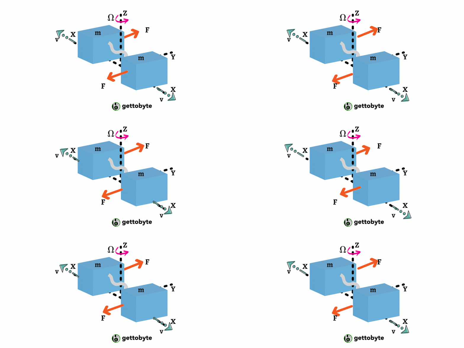
Coriolis Effect
The Coriolis Effect states that when a mass (m) moves in a specific direction with a velocity (v) and an external angular rate (Ω) is applied, the Coriolis Effect generates a force (F) that causes the mass to move perpendicularly. The value of this displacement is directly related to the angular rate applied.

Consider two masses oscillating in opposite directions at a constant frequency. When an angular rate is applied, the Coriolis effect produced by each mass is in opposite directions, resulting in a proportional change in capacitance between the masses. By measuring this change in capacitance, the angular rate can be calculated.
The MEMS sensor consists of a proof mass (i.e., it consists of 4 parts M1, M2, M3. M4) that continuously oscillates inward and outwards in the plane, thus causing a coriolis effect.
When the structure is being rotated, the Coriolis Force acts on the moving mass causing oscillations in the plane.
There are three modes depending upon the axis along which the angular rotation is applied:
- Roll Mode: When the angular rate is applied at the X-axis
- Pitch Mode: When the angular rate is applied at the Y-axis
- Yaw Mode: When the angular rate is applied at the Z-axis
What is MPU6050 IC
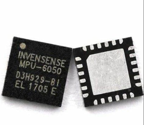 A MUST HAVE Motion Interfacing one finds in almost every smartphone and tablet. It is a 3-axis gyroscope and 3-axis accelerometer, in total an integrated 6-axis MotionTracking device all in a single small 4x4x0.9mm package. This package size has been achieved by the MEMS (MicroElectroMechanical System) innovation.
Coming to some technical aspect of the IC,
- It comes with a dedicated I2C sensor bus at 400KHz
- Features 3 16-bit analog-to-digital converters (ADC) each for digitizing gyroscope and accelerometer outputs.
- Gyroscope full-scale range of 250,500,1000 and 2000 degree/sec (DPS).
- Accelerometer full-scale range of 2g,4g,8g,16g and
- On-chip 1024 Byte FIFO buffer which enables the system to read the sensor data in burst and then enter the low-power mode.
- Lastly, it operates at a power supply voltage range of 2.375V – 3.46V.
Features of Accelerometer in MPU6050IC
The triple-axis MEMS accelerometer in MPU-60X0 includes a wide range of features:
- Digital-output triple-axis accelerometer with a programmable full scale range of ±2g, ±4g, ±8g and ±16g
- Integrated 16-bit ADCs enable simultaneous sampling of accelerometers while requiring no external multiplexer
- Accelerometer normal operating current: 500µA
- Low power accelerometer mode current: 10µA at 1.25Hz, 20µA at 5Hz, 60µA at 20Hz, 110µA at 40Hz
- Orientation detection and signaling
- Tap detection
- User-programmable interrupts.
GYROSCOPE FEATURES
The triple-axis MEMS gyroscope in the MPU-60X0 includes a wide range of features:
- Digital-output X-, Y-, and Z-Axis angular rate sensors (gyroscopes) with a user-programmable fullscale range of ±250, ±500, ±1000, and ±2000°/sec
- External sync signal connected to the FSYNC pin supports image, video and GPS synchronization
- Integrated 16-bit ADCs enable simultaneous sampling of gyros
- Enhanced bias and sensitivity temperature stability reduces the need for user calibration
- Improved low-frequency noise performance
- Digitally programmable low-pass filter
- Gyroscope operating current: 3.6mA
- Standby current: 5µA
- Factory calibrated sensitivity scale factor
Module of MPU6050
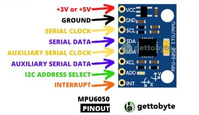
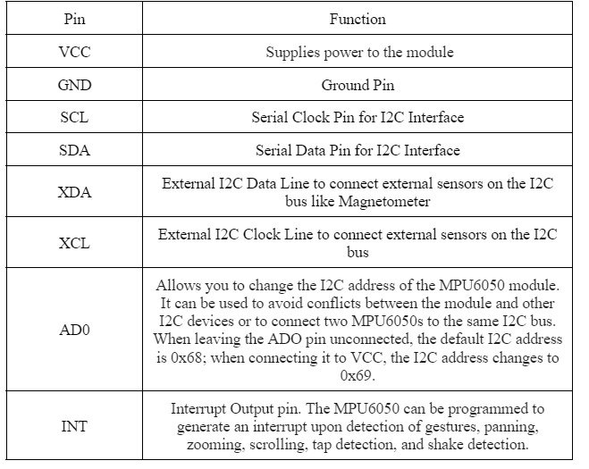
Block Diagram of MPU6050
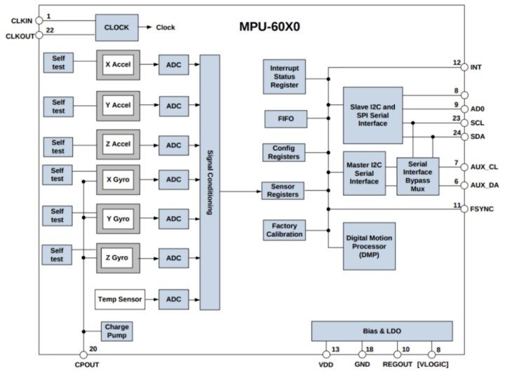
Three-axis MEMS rate gyroscope sensor with 16-bit ADCs and signal conditioning
It consists of three independent vibratory MEMS gyroscopes, which detect the rotation about the X, Y, Z axis. The capacitive change due to Coriolis Effect is observed whenever a rotation is caused about any of the axes. The corresponding signal is then amplified, demodulated and filtered to the corresponding voltage levels that relate to the angular rate. The sensor has an on chip 16 bit ADC to convert the signal voltage value to the corresponding digital value within the full range of DPS. The ADC sample rate is programmable from 8000 samples per second, down to 3.9 samples per second, and user-selectable low-pass filters enable a wide range of cut-off frequencies.
Three-axis MEMS accelerometer sensor with 16-bit ADCs and signal conditioning
As discussed the sensor has the suspended mass and acceleration along any axis includes the capacitive change placed between the suspended mass. When the device is placed on the flat surface, then values across X= Y= 0g and Z= g. It also consists of a dedicated sigma delta ADC for providing the digital outputs within the full range.
The DMP is used for computing motion processing algorithms which includes the data processing of the accelerometer, gyroscope. The output can be read from the FIFO buffer or from DMP’s register.
One interesting thing to note here is that the DMP has access to the MPU’s external pin, thus can be used to generate interrupts.
The purpose of DMP is to make the timing requirements and processing power divided from the host processor. This will help in achieving accurate results even with low latency.
The MPU-6050 communicates with the I2C protocol and always acts as a slave when communicating with the controller.
The voltage level for communicating with the master is set by the voltage on VLOGIC
The MPU-6050 has an auxiliary I2C bus for communicating with other 3rd party sensors. It operates on two modes:
- I2C Master Mode: Here, MPU6050 act as a master for the external sensor.
- Pass-Through Mode: Here the primary and auxiliary I2C buses are connected together allowing the controller to directly communicate with the external sensor.
A flexible clocking scheme allows internal and external clock sources for internal synchronous circuitry which includes ADC, DMP and various other control circuits and registers.
The internal source clock generation are:
- An internal relaxation oscillator
- Any of the X, Y, Z gyros (MEMS oscillators with a variety of 1% overtemperature)
The external clock sources are:
- 32.786 kHz Square Wave
- 19.2 MHz Square Wave
Consider a case where power consumption is a concern and the user wants to operate the data via DMP keeping gyros off. In such a case internal source is the best deal. But if the user wants gyros to be active then selecting gyros as clock source is a far better and more accurate option.
Remember, clock sourcing is an important parameter as the timing error will be reflected in calculation and performance by DMP.
The read only register, with the updated values of accelerometer, gyro, auxiliary sensor and temperature, the serial data register is accessed by the serial interface.
The sensor consists of 1024 bytes of FIFO register, again accessible via a serial interface. The FIFO buffer tracks and validates the data bytes contained in FIFO, hence determining the data written for gyro, accelerometer, temperature and auxiliary sensor readings into the FIFO.
Interrupt functionality is configured via the Interrupt Configuration register. Items that are configurable include the INT pin configuration, the interrupt latching and clearing method, and triggers for the interrupt. Items that can trigger an interrupt are
- Clock generator locked to new reference oscillator (used when switching clock sources);
- New data is available to be read (from the FIFO and Data registers);
- accelerometer event interrupts; and
- The MPU-60X0 did not receive acknowledgement from an auxiliary sensor on the secondary I2C bus.
An on-chip temperature sensor and ADC help to measure the sensor die temperature which can be read from FIFO or Sensor Data Register.
It generated the internal supply, reference voltage and current required by the module. The two inputs are unregulated VDD of 2.375 to 3.64V and VLOGIC range from 1.71 to VDD. The LDO output is bypassed by the capacitor at REGOUT.
It generates the high voltage required for the MEMS oscillations whose output is bypassed by a capacitor at CPOUT.
Auxiliary and Primary I2C connection
The Sensor is connected to the MCU (system Processor) via I2C bus lines i.e., SDA and SCL along with the external compass sensor as shown. The module has an inbuilt bypass multiplexer, which connects the primary I2C bus pins 23 and 24 with the auxiliary sensors I2C pins 6 and 7.
Once the auxiliary sensors have been configured by the system processor, the interface bypass multiplexer should be disabled so that the MPU-6050 auxiliary I2C master can take control of the sensor I2C bus and gather data from the auxiliary sensors.

How does MPU6050 communicate with the host?
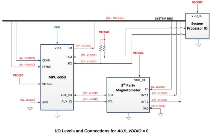
A two wire, half duplex interface comprising Serial Data SDA and Serial Clock SCL, I2C lines are in general open-drain and bi-directional.
It is a master slave implementation where the master puts the slave device address on the bus and salve with the matching address acknowledges the master.
Here the MPU-6050 operates as a slave device when communicating with the MCu and the SDA and SCL lines are pulled up to VDD. The maximum bus speed is 400kHz.
The slave address of the MPU-6050 id 0b110100x, a 7-bit long. Here the LSB bit i.e.x in the 7-bit long address is determined by the logic level at AD0 pin.If x=0 i.e., pin AD0 is Logic LOW otherwise Logic HIGH.
The I2C communication begins and ends with the START and STOP COndition respectively. Whenever the master puts the Start condition on the bus the communication is established and as long as the Stop condition is sent by the master
The transaction of HIGH too LOW for the SDA pin keeping the SCL pin HIGH is marked as the Start condition.
The transaction of LOW too HIGH for the SDA pin keeping the SCL pin HIGH again is marked as the Start condition.

The data format of the I2C is 8-bit long. The transmission byte is followed by the acknowledge signal (ACK) shock clock generated by the master. The slave sends the ACK signal by pulling the SDA down and holding it during the HIGH portion of the acknowledged clock pulse.
If a slave is busy and cannot transmit or receive another byte of data until some other task has been performed, it can hold SCL LOW, thus forcing the master into a wait state. Normal data transfer resumes when the slave is ready and releases the clock line.
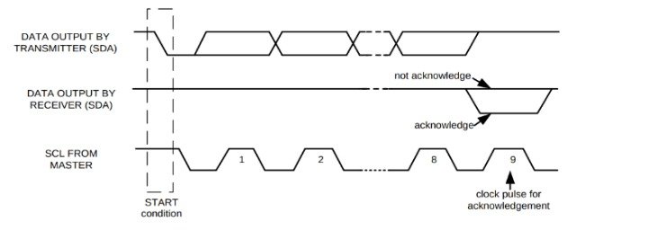
Coming to the communication part, the master first sends the Start condition followed by the 7-bit address with 8th bit being read/write bit. The read/write signifies whether the master wants to read the data or to send the write command. The 9th clock pulse consists of the ACK or NACK (not Acknowledged) signal. The data transmission is terminated by the Stop Condition.
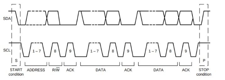
Interestingly the master can send Start condition and address to slave without first generating the Stop condition. 
For Writing the internal MPU-6050 register, the master first sends the Start Condition followed by the slave address and writes bit 0. At the 9th clock pulse, the slave sends the ACK signal. Seeing ACK, master sends the register address to the bus on whose data master wants to write which is again followed by the ACK signal from the slave. After that the master puts the register data on to the bus. The communication eds with the Stop Condition sent by the master.
To write multiple bytes after the last ACK signal, the master can continue outputting data rather than transmitting a stop signal. In this case, the MPU-60X0 automatically increments the register address and loads the data to the appropriate register.

To read the internal MPU-60X0 registers, the master sends a start condition, followed by the I2C address and a write bit, and then the register address that is going to be read. Upon receiving the ACK signal from the MPU-60X0, the master transmits a start signal followed by the slave address and read bit. As a result, the MPU-60X0 sends an ACK signal and the data. The communication ends with a not acknowledged (NACK) signal and a stop bit from the master. The NACK condition is defined such that the SDA line remains high at the 9 th clock cycle. 

Alternative to MPU6050
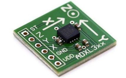
The ADXL335 (Adafruit Industries) is a thin, small, low power, complete 3-axis accelerometer with signal conditioned voltage outputs. It measures acceleration with a minimum full-scale range 3g. This device measures the static acceleration of gravity in tilt-sensing applications and dynamic acceleration resulting from motion, shock, or vibration. The ADXL335 contains a polysilicon surface micro machined structure built on top of a silicon wafer. Polysilicon springs suspend the structure over the surface of the wafer and provide resistance against acceleration forces. A differential capacitor, consisting of independent fixed plates attached to the moving mass, measures the deflection of the structure. Acceleration unbalances the capacitor, which, in turn, results in a sensor output with amplitude proportional to the acceleration experienced.
Adding a 3-axis magnetometer to a 3-axis accelerometer and a 3-axis gyroscope

will obtain a 9-axis inertial measurement unit (IMU) sensor which provides 9DoF plus roll, yaw, and pitch information during motion and orientation of the hand. Magnetic field sensor is a small-scale microelectromechanical systems(MEMS) device for detecting and measuring magnetic fields (Magnetometer). According to InvenSense, “Gyro noise performance is 3× better, and compass full-scale range is over 4× better than competitive offerings.” The MPU-9250 uses 16-bit Analog-to-Digital Converters (ADCs) for digitizing all nine axes, making it a very stable 9 Degrees of Freedom (DoF) board. 


