What is ADC peripheral in Microcontroller?
- An ADC (Analog to Digital Converter) is a peripheral in microcontrollers that converts an analog voltage to a numerical value. It allows the microcontroller to accept analog sensor outputs and convert them into the digital domain
ADC Peripheral important concepts
–> Now to understand how ADC peripherals are used in microcontrollers it is important to understand the following concepts:
> Types of ADC
–> Multiple ADC types exist like SAR(Successive Approximation Register) ADC, FLASH ADC, SIGMA-DELTA ADC (Σ-Δ), DUAL-SLOPE ADC, and more. but you might prominently see FLASH ADC, SIGMA-DELTA ADC, and SAR ADC. If I have to compare them among themselves then first we need to know for what parameter an ADC is considered as best. Parameters are:
- Speed
- Accuracy
- Power Efficiency
–> Now to conclude above mentioned common ADC with these parameters, you can get a great balance of all three parameters is SAR ADC, where FLASH ADC gives the fastest conversion but with the price of power consumption and accuracy, similarly, Sigma Delta ADC (ΣΔ) gives best accuracy but at the cost of conversion speed and power efficiency.
> ADC Counter and Reference Voltage
–> After talking about the types of ADC, we need to know about the resolution of ADC. You can compare this ADC resolution with the camera resolution and understand the concept. just like in the camera, a higher resolution image provides more detailing to the photo, similarly, more resolution in ADC provides a more detailed conversion. Resolution of ADC determines that in how many different voltage levels can be defined. Consider a 5V signal, now if I ask you to divide it into 3 different levels then you might give me 0V, 2.5V, and 5V. Now these 3 levels of signal can provide me with more flexibility to operate rather than only two states(0V and 5V). Similarly, more levels provide more control over the signal to use it for various purposes. Resolution in ADC is measured in “bit”. Like 8-bit ADC, 10-bit ADC, 12-bit ADC, or 16-bit ADC. To calculate the number of levels an ADC can generate, we use below mentioned formula:

–> Now these levels can have individual voltage values depending on their Reference Voltage. By remembering the Reference Voltage, we need to understand “what a reference voltage is in ADC?”. As the term is pretty much self-explanatory, it is a voltage level for bounding the upper and lower limit of ADC. Usually lower limit of any ADC is tied internally with the MCU’s ground reference. Talking about the upper limit, it can vary as per user requirement as well and it is also tied to the VCC of MCU(in case of user doesn’t need an external supply for ADC reference). Let’s say ADC is tied with 5V Reference Voltage, then you can calculate the voltage of every level offered by your ADC. Taking the very same 5V reference with 10-bit ADC. Now to calculate the voltage per level you just need to divide the reference voltage by the total number of levels offered in ADC.

> ADC Clock
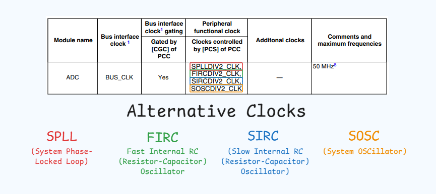
–> ADC as being peripheral, it is also attached to the clock of the system for working. You can always customize the clock period of the ADC peripheral by choosing a different clock and prescalar. Prescalar is a specific value that divides the clock into desired frequencies. Let’s say you option of clocks – 5MHZ, 12MHz, 20MHz, and 80MHz. But you need a clock of 10MHz, there you can take the help of Prescalar to divide the 20MHz clock by 2.
NOTE: Remember, Prescalar can only divide the clock, you cannot multiply a 5MHz clock with 2 to generate 10MHz.

> ADC Sample Time and Calibration
–> Now, it is time to understand Configurable Sample Time, Before going to Configurable Sample Time, we need to know about Sample Time, Sample Time is the number of ADC Clock Cycles for which input samples are taken. To understand this clock cycle, let’s take a simple example and understand it. consider a clock with a frequency of 1KHz then calculate its one-clock cycle time, you just have to reciprocate the frequency, in our case, which will be 1/1000Hz = 1ms which means a single ADCK clock cycle is 1ms. Range of Configurable Sample Time is 1-255. Now you get the understanding of how Configurable Sample TIme works, in our condition if I use 255(Maximum value of Configurable Sample Time) then for 255 ADCKclock cycle = 255 ms meaning one single ADC conversion is done by sampling the analog signal for 255ms. Taking a lower sample time increases the overall conversion time of ADC.
–> Self-Calibration is a technique to refresh and remove unwanted parameters that can affect the accuracy of ADC conversion. Self-Calibration is always recommended just after the initiating ADC and before starting conversion. Some MCUs make this calibration mandatory and some make it optional.
> ADC Channels/ADC pins and ADC Instances
–> ADC Instances represent the number of ADC peripherals available to your development kit. ADC Channels/Pins denote the input analog pins attached to the ADC peripheral. Let’s understand this with examples of different development boards.
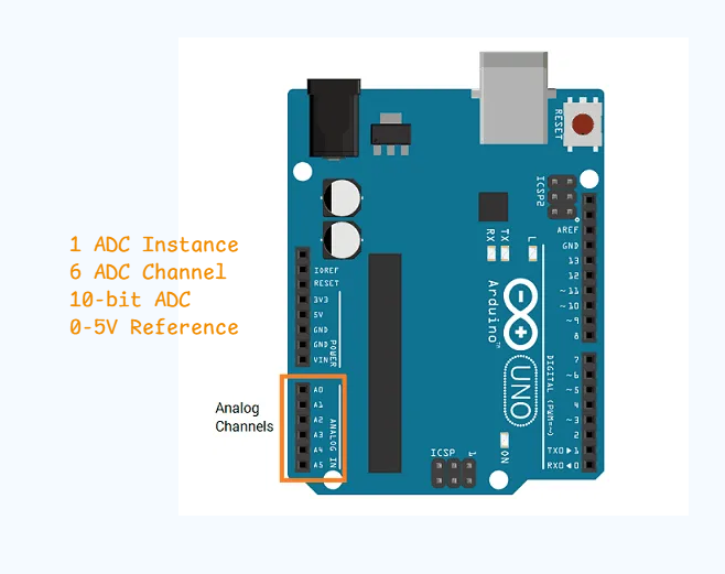
- Arduino UNO

- As we can read, 1 ADC Instance which means only a single ADC is available for conversion.
- 6 ADC Channel means six pins can be used for analog signal inputs.
- 10-bit ADC means that it can generate 1024 different voltage levels.
- 0V-5V is the reference voltage meaning this is the operating upper limit that can be used.
- STM32F103

- This MCU offers 2 separate ADC Instances where we can use 2 separate ADC for different analog inputs.
- 10 ADC Channels multiplexed between 2 ADC Channels.
- 12-bit ADC means that it can generate 4096 different voltage levels.
- 2.4V-3.6V is the reference voltage meaning this is the operating upper limit that can be used.
> ADC Start (ADC Triggering)
–> In ADC systems, triggers are signals that start the conversion process for the complete ADC block(ADC0 or ADC1), while by pre-triggers we mean the ADC channels of the ADC instance, whose conversion has to be done before the conversion of the whole ADC instance begins. Now there are 2 types of ADC Triggers in S32K1xx MCU:
- ADC Software Trigger: By writing some bit value to ADC Peripheral Register, after that ADC conversion is started.
- ADC Hardware Trigger: By configuring some external ADC hardware event and after that ADC conversion starts.
> ADC Conversion Mode (Single and Continuous)
–> Through conversion modes, we understand which type of conversion we want whether it should be continuous or one at a time.
- Let’s assume you have a condition where you want to convert analog to digital signal consistently and check whether it surpasses the threshold value or not. In this specific condition, you fastest conversion without any delay, this condition can be fulfilled with the Continuous Conversion Mode of ADC where you have to start the ADC once then the conversion will automatically take place at the speed of the ADC clock input(which can be varied).
- To understand the Single Conversion Mode, let’s consider another condition where you have to read the analog value at a specific time interval(like every 2 min or 5 min) where the threshold comparing is a period in time. Then you assign this role to some other peripheral, which calculates this time period for you and then invokes a request to ADC peripheral for conversion. These require the Single Conversion Mode of ADC peripheral where conversion needs to take place only when needed.
> ADC Data Sampling via Polling/Interrupts and DMA
–> Polling Technique: In this scenario, the user has to read the result of the conversion by bit shifting in application code for continuous conversion.
–> Interrupt Technique: In this scenario, the user can convert all this register result reading and bit shifting assigned to ISR of ADC for seamless application and also Interrupt provides an extra notification feature to detect the conversion.
–> DMA: Completing all the unnecessary workload through DMA peripheral where DMA controls CPU load and extra memory/register.
> ADC Averaging and Threshold Features
–> ADC Averaging provides an additional feature to this peripheral where an average of sampled conversions can be done through back-end hardware without any firmware support. For example, I take the hardware average as 32 samples where 32 conversions are collected together and then averaged by hardware after which it is flushed in the result registers.
–> Threshold features provide a very interesting result bounding system, where you can have an upper or lower bound of result stored, and whenever your conversion crosses over or under the upper or lower bound mentioned.
