
General Purpose Input/Output(GPIO) is a crucial peripheral in microcontrollers, enabling interaction with the external world by sending and receiving digital signals.

Digital Signals, here are referenced as High and Low Signals. High signal is +5/+3.3V level and Low Signal is 0V level. As MCU’s are digital devices, so it can only understand High and Low Voltage levels.
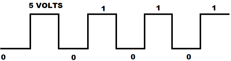
Almost all the pins of the Microcontroller are by default part of the GPIO peripheral, accept from the power pins. Every Pin can be configured in Input or Output State.
State of Pins
- When a pin is configured as Input State, it can detect the level of external signal whether it is high signal or low signal. For example when we press the button, MCU process that as a external signal.
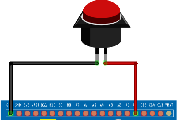
GPIO as Input signal
Button is connected to one of the GPIO pins of the Microcontroller, which is being configured as Input state and when we press the button a High or Low voltage signal is generated. Which voltage level is generated? is detected by the configured GPIO Pin.
- When a pin is configured as Output State, it can generate the High Signal or Low Signal to drive the external electronic devices. For example, LEDs are electronic devices which needs High signal to power-on them and low signal to power-off them.
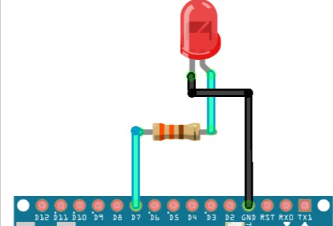
GPIO as Output signal
So LEDs are connected to one of the GPIO pins of the Microcontroller, which is being configured as Output State and then by programming we can configure the signal that has to be generated from the corresponding configured GPIO pin.
Input/output are defacto states of pins, apart from these 2 there are other states too, on which pins can be configured.
State of pins can be:
- Output
- Input
- PullUp
- PullDown
- Tri-state
GPIO pins categorization
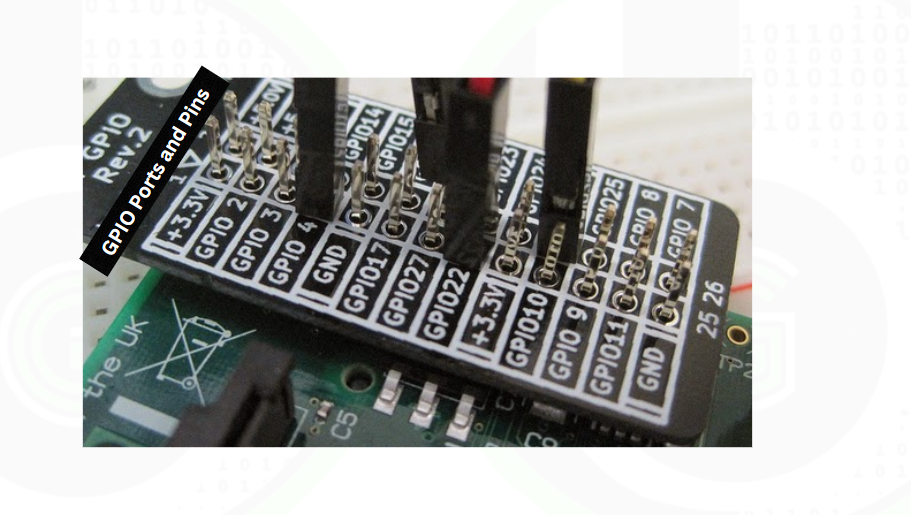
GPIOs are organized into banks, each requiring a unique identifier to identify a specific pin. These identifiers are commonly referred to as “Ports” and “Pads”. With the vast number of pins available on a microcontroller, it is essential to have a mechanism to reference and utilize them effectively.
To simplify this process, GPIO pins are now divided into Ports, with each Port containing a multiple of 8 pins. This division allows for easy referencing and addressing of the pins on the microcontroller.
By utilizing this system, developers can efficiently access and manipulate the GPIO pins on a microcontroller, streamlining the development process and improving overall functionality.
In S32K144 MCU, there are 5 ports of GPIO: named as PTA to PTE. Each Port pin has 16 pins.
In S32K144 reference manual, GPIO peripheral is being dicided into 2 modules: PORT (Port Control and Interrupt Module) and GPIO (General Purpose Input/Output Module).
PORT Module is responsible for Interrupt and Port Control Operations (Like alternate functions, Pull-up/down, drive strength) of the above Ports specified. GPIO module is responsible only for Controlling Input/Output directions of the port pins.
Features of GPIO in S32K144 MCU
- Pins can be configured as Output.
- Pins can be configured as Input.
- Pins support the multiplexing of signals, so that a single pin can be do different job(refer to signal multiplexing section).
- Dedicated Port Output registers for set/clear/toggle the bits.
- Efficient bit manipulation of the general-purpose outputs is supported through the addition of set, clear, and toggle write-only registers for each port output data register.
- GPIO module can operate on 3 modes: Run Mode, Stop Mode and Debug Mode
- GPIO Module is clocked by System clock.
- GPIO module has a feature of Lock feature, in this feature we can lock the Mode of operation of PIN in one Power Cycle.
Registers of GPIO in S32K144
For simplicity, each GPIO port’s register appear with the same width of 32 bits, corresponding to 32 pins. The actual number of pins per port in S32K144 is 16 pins. So we will be addressing only first 16 bits of the registers, on last remaining 16 bits are irrelevant for us. But in S32K144 there are 16 pins only per port, so we will be accessing only first 16 bits of the registers (0-15), reading & writing on (16-31) will have no effect.
In S32K144, there are registers to support 8bit, 16-bit and 32-bit access. Registers of GPIO:
- GPIO Data Direction register: Direction of GPIO pin
- GPIO output data register: Output direction of GPIO pin
- GPIO Input Data Register: Displays the logic value on each pin
Efficient bit manipulation of the general-purpose outputs is supported through the addition of set, clear, and toggle write-only registers for each port output data register.
Each Port of GPIO has 16 pins. And each pin is referenced as each bit of the above registers.
Features of Pin configured as Output:
Output: Pin is configured for the GPIO Function and corresponding port data direction register bit is set.
For efficient bit manipulation, there are dedicated output registers for toggling, Set High or Set LOW the pins. Instead of doing the manipulation of pin signals via software using bit manipulation and shifting
Features of Pin Configured as Input
Input: If Pin is configured for the GPIO function and the corresponding port data direction register bit is clear.
S32K144 MCU comes in 3 pin counts: S32K144_100lqfp, S32K144_64lqfp, S32K144_48lqfp. The one which we will be using is S32K144_100lqfp. S32K144 EVB board which is explained in last blog, has S32K144 MCU of S32K144_100lqfp packaging. 

For GPIO peripheral to use, in terms of Hardware first thing that is needed is pinout of the MCU.
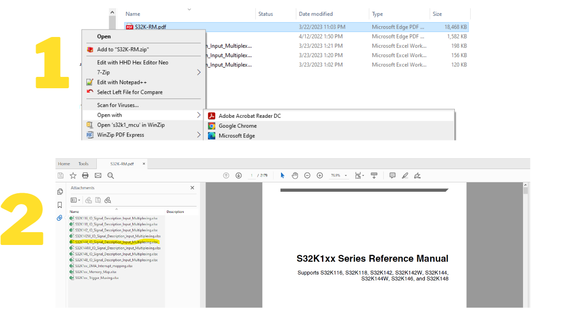
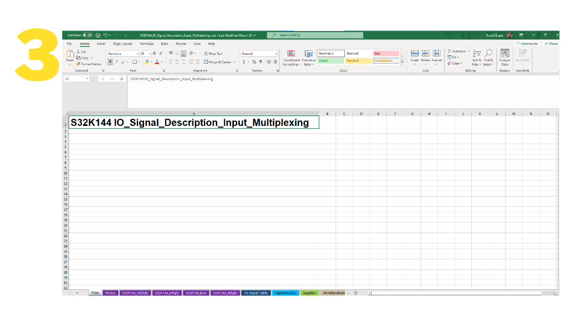
To see the pinout of S32K144 MCU, you will not find that on its Datasheet or Reference Manual. But there is separate excel sheets to know details for its pinout, by the name of: S32K144_IO_Signal_Description_Input_Multiplexing.excel.
This excel is attached with S32K144 MCU reference manual. Open the Reference Manual of S32K144 with Adobe Acrobat and click on below highlighted icon. 
Now coming back to pinout of S32K144 MCU, this below is the pinout that is extracted from the excel sheet for the S32K144_100lqfp packaging. We would be referring this packaging only throughout the series,
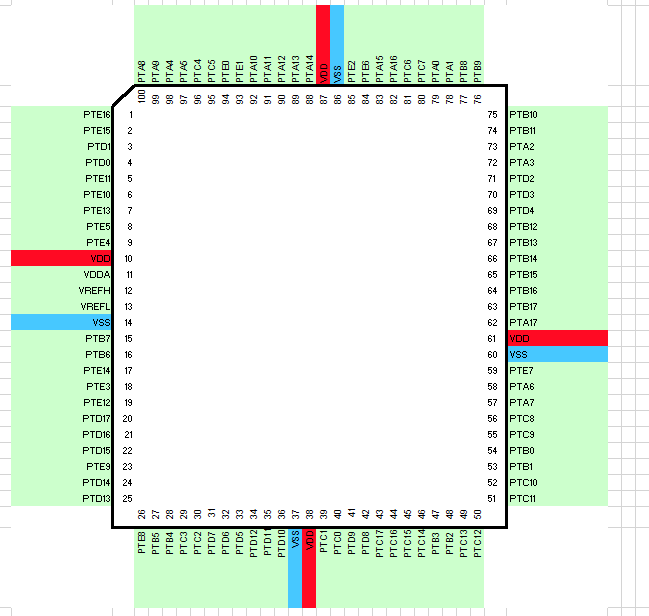
One can see, that their are 100 pins in this MCU S32K144. Starting from pin 1 which belongs to PTE16 and pin 100 which belongs to PTA8.
As you can see there are so many, to use them we need to have some kind of referencing. Thus, concept of Ports is there. Their are total 5 Ports in S32K144 MCU and supply pins:
- PTA: PTA0-PTA17(18 pins)
- PTB: PTB0-PTB17(18 pins)
- PTC: PTC0-PTC17(18 pins)
- PTD: PTD0-PTD17(18 pins)
- PTE: PTE0-PTE16(17 pins)
- And 11 Supply pins (VDD, VDDA, VREFH, VREFL, VSS)
Now in the excel sheet one can find that there are multiple sheets as follows.
In this section, pins description according to MCU packaging and pin count size is listed.
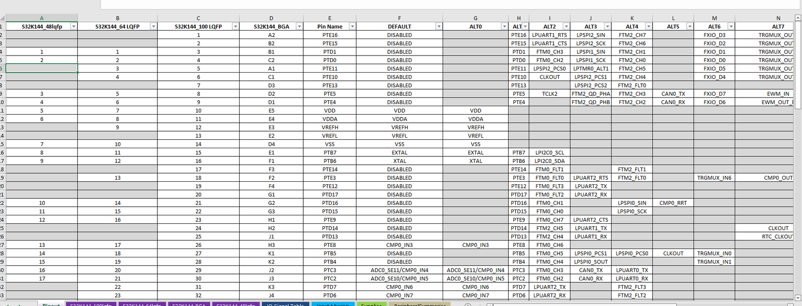
Next 3 sections have the MCU pinout photo for the different packaging sections
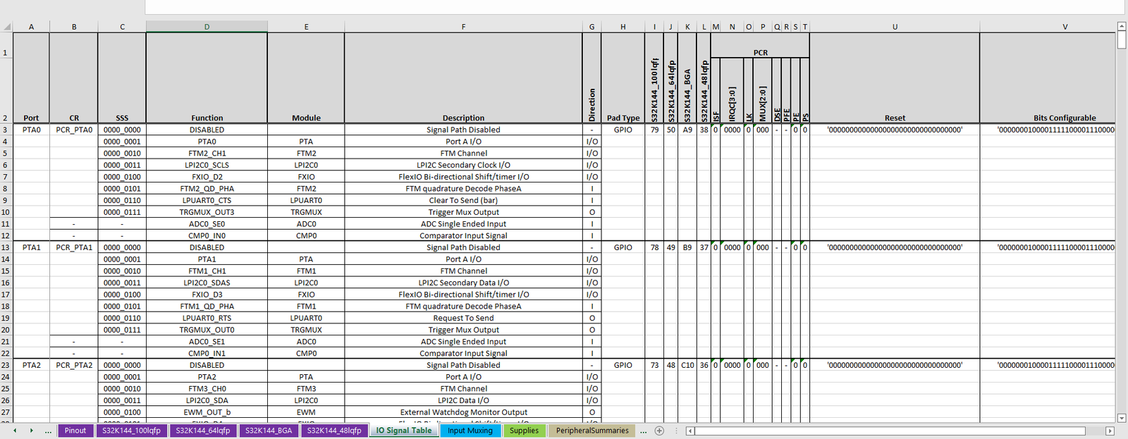
In this section, in detail description for each Pin is there. Parameters like what all alternate functions that pin can have, its reset value, its direction, description and various other parameters are listed.
In this sheet, what all pins are there for specific peripheral pins. This sheet makes quite easy to figure which pin can be used for corresponding peripheral pins.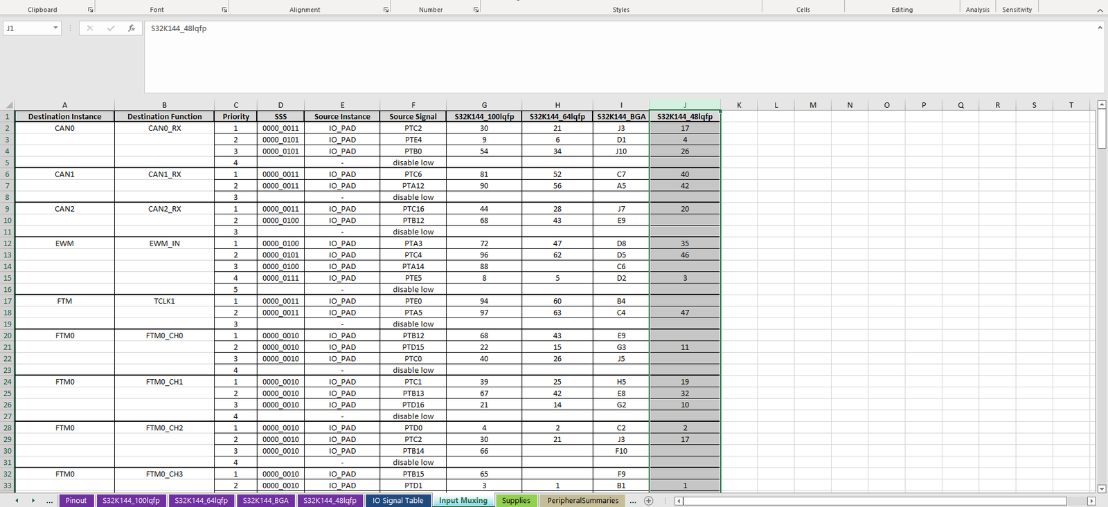
This sheet, has information about the supply pins of the MCU. Their are total 11 supply pins in S32K144 MCU.
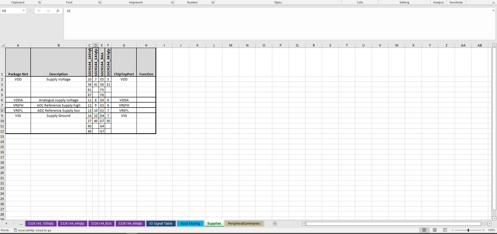
This sheet summarizes what all pins are there are each peripheral.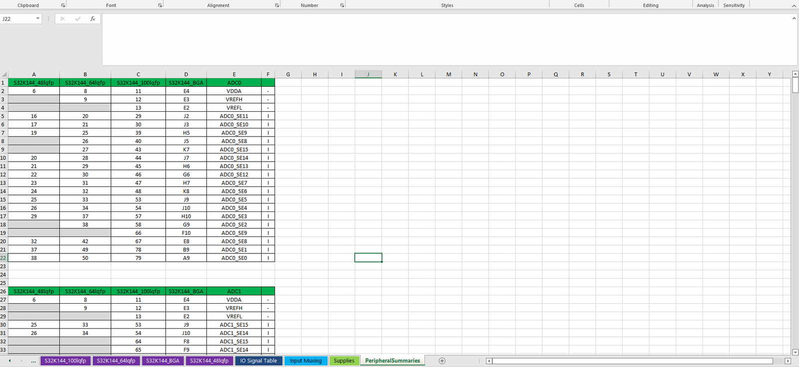
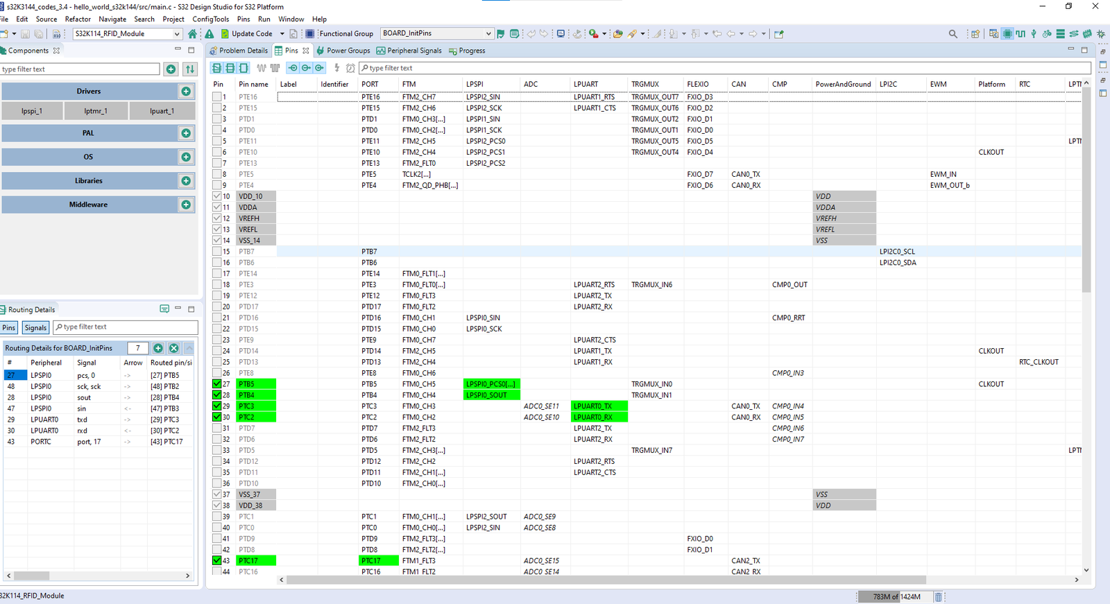
Also in S32 Configuration Tool in S32 Design Studio one can see all the details of the MCU Pinout and description.( Will be telling more on S32 Configuration and S32 DS later.)
Now in S32K144 EVB Board, pin numbering is done in bit different way. Pin Naming is not done directly by the name of Pins name as referenced in Pinout Sheet. Instead, it is done in terms of Jacks. As shown in below pic.
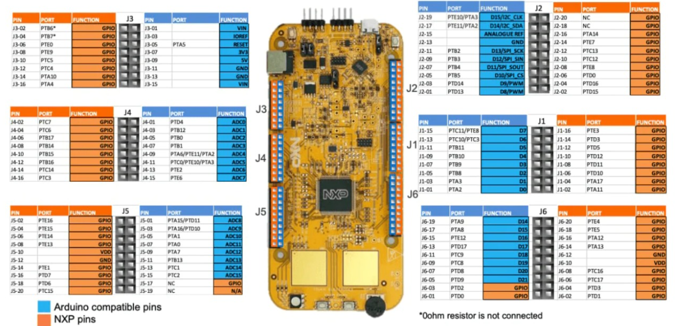
There are 6 Jack Connectors: J1-J6. All Jack are of Female Connectors(This might make the connections messy). J1 & J3 have 16 pin count. J5, J6 & J7 have 20 pin count. J4 have 15 There are. From the above pic you can refer out the Pin name of each Jack Pin. And then correspondingly get to know about that Pin via Sheet.
S32 SDK/ drivers provide an easy to use and quick way to use the GPIO peripheral in S32K144, which is known as Pin Driver. 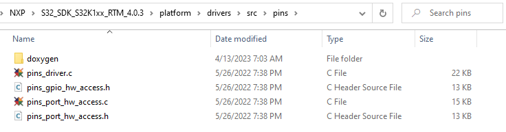
Each S32 SDK driver can be configured and enabled to use in the project via S32 Configuration Tool. Will be digging into that part, in next section. For now, let’s understand the Pin driver in more details, so as to use the GPIO periperal.
Broadly there are 5 files in Pin Driver, that controls the GPIO peripheral in S32K144 MCU:
- pins_driver.h
- pins_driver.c
- pins_gpio_hw_access.h
- pins_port_hw_access.h
- pins_port_hw_access.c
pins_driver.h & pins_driver.c are the GPIO Peripheral Abstraction Layer and Rest 3 are the GPIO low-level drivers of the GPIO peripherals.
GPIO Peripheral Abstraction layer functions are the ones that are directly used in main.c or Application code. And internally these functions use the GPIO low-level driver functions.
Thus, we would find that in Rest 3 files, most of the functions are static functions and static inline functions, as low-level driver functions are internally used in Peripheral Abstraction Layer functions. So that if hardware is changed, so only low-level driver functions would be changed. GPIO PAL functions would remain same and their would be very small amount of change required in Application code or main.c. This is how Code Portability and modularity is designed, providing efficient use.
Configuring GPIO Pins
First thing, that we need to do for using GPIO pins, is to configure them. By configure we mean:
- Which pin to use and that pin belongs to which port.
- pin to be used in what state or if pin to be used by other peripheral then configuring the state of pin according to that(pin multiplexing)
- to configure the features, like pullup/down resistors, slew rate, open drain, over current and etc( this is kind of chip specific, according to the chip their are different features)
To configure the GPIO pins, in pins_driver.h there is a structure pin_settings_config_t. This structure allows users to properly exploit S32K1 GPIO features.