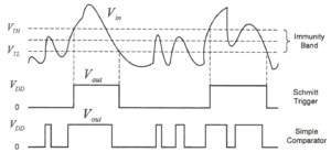
A SCHMITT TRIGGER is a device which uses a voltage comparator to convert a noisy or slow signal edge into a clean and desirable edge instantaneously.
For a real time system, the external signals do not change instantly, due to slower slew rate which depends on inheritance parasitic capacitance, resistance or an inductor at the input side.
As the processor chip has a Schmitt Trigger, it increases the slew rate and increases the noise immunity for the signals which are captured.
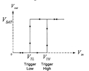
Let us understand the implementation of the Schmitt Trigger. It consists of a voltage comparator with positive feedback. The output Vout depends between two input voltage V+ and V–. If V+ > V–, Vout is quickly saturated to VSAT, otherwise Vout = 0
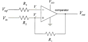 For an ideal op-amp, the current flowing through resistor R3 is zero and thus we have
Vref = V–
The op-amp output Vout has two saturation values, as shown below
Vout = VSAT if V–
0 if V– < V+
However, V+ depends on Vout and Vin· Therefore, Vout depends on both the input Vin and
the recent history of Vout· Such an effect is called hysteresis.
Using KCL, assuming that the current flow in the non inverting input terminal of op-amp is zero,
Vin – V+ /R2 = V+ – Vout / R1
On solving the above equation we will get,
Vin = R2Vout + R1Vin / R1 + R2
At the time instant when Vout transits from one saturation value to the other saturation value, we have
V+ = Vref
Thus,
Vref = R2Vout + R1Vin / R1 + R2
Solving further we get,
Vin = (1 + R2/ R1)Vref – (R2/R1)Vout
As discussed earlier, Vout has only two possible values. If Vout = 0 initially and Vin
increases, we can obtain the trigger high threshold VTH at which Vout transits to VSAT:
VTH = (1 + R2/R1) Vref – (R2/R1)*0 = (1 + R2/R1)Vref
On the other hand, if Vout = VSAT initially and Vin decreases, we can obtain the trigger low threshold VTL at which Vout transits to 0:
VTL = (1 + R2/R1) Vref – (R2/R1)VSAT
Vout can be determined by comparing it with two thresholds VTH and VTL.
When Vin climbs through VTH , Vout is rapidly switched to the upper limit VSAT· Conversely, once Vin falls below VTL, Vout makes a transition to the lower limit.
Note that VTH > VTL , i.e., the threshold for switching to high is greater than the threshold of switching to low.
A Schmitt trigger when compared,
- Provide a better boise rejection.
- Larger threshold for switching high and low for switching.
- Immune to undesired noise.
The SLEW RATE of a GPIO pin is the speed of change of output voltage with respect to unit time.
Slew Rate = ΔV/ Δt
In simple words, If the GPIO pin changes from LOGIC LEVEL 0 to LOGIC LEVEL 1, the voltage changes from 0V to 5V in just 5µs, then the slew rate is simply 1V/µs.
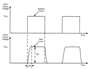
The higher the slew rate, the shorter time the output voltage takes to rise or fall to desired values. Therefore, a higher slew rate allows faster speed at which the processor can toggle the logic level of a GPIO pin. A shorter rise and fall time allows a GPIO pin to change its logic value more rapidly.
A high slew rate can result in significant electromagnetic interference (EMI), also known as radio frequency interference (RFI), to nearby electronic circuits. This is due to the large-amplitude and high-frequency harmonics produced by a fast-rising and falling signal, which can cause malfunctions in a victim circuit through radiation, conduction, or induction. To reduce EMI disturbance, a slower slew rate is generally preferred.
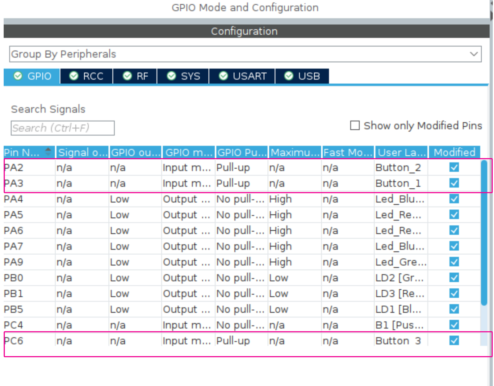
The port bit of GPIO can be configured by the software depending upon the hardware characteristics in various modes such as:
- Input floating
- Input pull-up
- Input-pull-down
- Analog
- Output open-drain with pull-up or pull-down capability
- Output push-pull with pull-up or pull-down capability
- Alternate function push-pull with pull-up or pull-down capability
- Alternate function open-drain with pull-up or pull-down capability
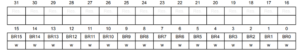
Each I/O port bit is freely programmable, however the I/O port registers have to be accessed as 32-bit words, half-words or bytes. The purpose of the GPIOx_BSRR register is to allow atomic read/modify access to any of the GPIOx_ODR registers. In this way, there is no risk of an IRQ occurring between the read and the modify access.
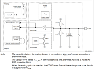
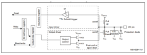
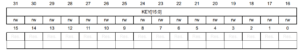
The above diagram shows the basic structure of a Three-volt tolerant (TT) and Five-volt tolerant (FT) I/O port bit.
During and just after reset, the alternate functions are not active and most of the I/O ports are configured in analog mode.
The debug pins are in AF pull-up/pull-down after reset:
- PA15: JTDI in input mode with pull-up
- PA14: JTCK/SWCLK in input mode with pull-down
- PA13: JTMS/SWDAT in input mode with pull-up
- PB4: NJTRST in input mode with pull-up
- PB3: JTDO in Hi-Z mode no pulls
PH3/BOOT0 is in input mode during the reset until at least the end of the option byte loading phase.
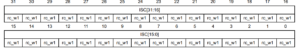
A Multiplexer allows the one peripheral Alternate Function to an I/O pin at a time thus reducing the conflict between the available different peripherals available at same I/O.
I/O pins have up to 16 Alternate Functions i.e., AF0 toAF15 which are controlled via GPIOx_AFRL (AF0 to AF7) and GPIOX_AFRH (AF8 to AF15).
Following is the I/O configuration
- DEBUG FUNCTION: when the device RESET, these pins are assigned as Alternate Function pins which are accessed by Debugger Host.
- GPIO: configure the I/O as Output, Input or Analog using GPIOx_MODER.
- PERIPHERAL ALTERNATE FUNCTION:
- Connect the I/O to the desired AFx in one of the GPIOx_AFRL or GPIOx_AFRH.
- Select the type, pull-up/pull-down and output speed via the GPIOx_OTYPER, GPIOx_PUPDR and GPIOx_OSPEEDER registers, respectively.
- Configure the desired I/O as an alternate function in the GPIOx_MODER register.
- ADDITIONAL FUNCTION:
- For functions like ADC, COMP, configure I/O as Analog Mode in GPIOx_MODER by enabling ADC and COMP registers.
- For functions like RTC, WKUPx and oscillator, configuring their registers is also needed along with setting higher priorities over other GPIO registers.
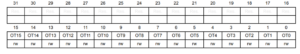
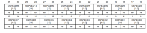
- GPIO ports have 4 32 bit MEMORY-MAPPED Control Registers (GPIOx_MODER, GPIOx_OTYER, GPIOx_OSPEEDR, GPIOx_PUPDR) to configure up to 16 I/Os.
- GPIOx_MODER: select the I/O mode.
- Output
- Input
- Analog
- Alternate Function
- GPIOx_OTYER: select the Output Type
- Push-Pull
- Open Drain
- GPIOx_OSPEEDR: select the speed
- Low
- Medium
- Fast
- High
- GPIOx_PUPDR: select the Push-Up or Pull-Down whatever the I/O direction
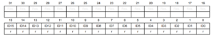
Each GPIO has 2 16-bit MEMORY-MAPPED Data Register.
- GPIOx_IDR: Input Data Register
- Read-Only register
- Stored the Input data
- GPIOx_ODR: Output Data Register,
- Read/Write register
- Stored the Output data
GPIOx_BSRR: Bit Set ResetRegister is a 32-bit
- Allows the application to Set and Reset each individual bit in the GPIOx_ODR. The bit set reset register is twice the size of GPIOx_ODR.
- To each bit in GPIOx_ODR, correspond two control bits in GPIOx_BSRR: BSH and BRL
- When writing ‘1’ bit BSL Sets the corresponding ODR bit
- When writing ‘1’ bit BSH Reset the corresponding ODR bit
- Writing ‘0’ does not affect the corresponding ODR bit
- If there is an attempt to both set and reset a bit in GPIOx_BSRR, the set action takes priority.
GPIOx_LCKR: Lock Register used to Lock or Freeze the GPIO Control.
The registers which are locked are:
- GPIOx_MODER
- GPIOx_OTYPER
- GPIOx_PUPDR
- GPIOx_OSPEEDR
- GPIOx_AFLR and GPIOx_AFHR
This register is used to lock the configuration of the port bits when a correct write sequence is applied to bit 16 (LCKK). The value of bits [15:0] is used to lock the configuration of the GPIO.
During the write sequence, the value of LCKR[15:0] must not change.
When the LOCK sequence has been applied on a port bit, the value of this port bit can no longer be modified until the next MCU reset or peripheral reset.
When the I/O port is programmed as input:
- The output buffer is disabled
- The Schmitt trigger input is activated
- The pull-up and pull-down resistors are activated depending on the value in the GPIOx_PUPDR register
- The data present on the I/O pin are sampled into the input data register every AHB clock cycle
- A read access to the input data register provides the I/O state

When the I/O port is programmed as output:
- The output buffer is enabled:
- Open drain mode:
- ‘0’ in the Output register activates the N-MOS
- ‘1’ in the Output register leaves the port in Hi-Z
- Open drain mode:
Note: In this case P-MOS is never activated
- Push-pull mode:
- ‘0’ in the Output register activates the N-MOS
- ‘1’ in the Output register activates the P-MOS
- The Schmitt trigger input is activated
- The pull-up and pull-down resistors are activated depending on the value in the GPIOx_PUPDR register
- The data present on the I/O pin are sampled into the input data register every AHB clock cycle
- A read access to the input data register gets the I/O state
- A read access to the output data register gets the last written value
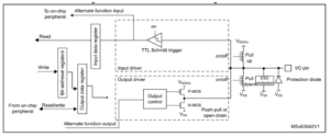
When the I/O port is programmed as alternate function:
- The output buffer can be configured in open-drain or push-pull mode
- The output buffer is driven by the signals coming from the peripheral (transmitter enable and data)
- The Schmitt trigger input is activated
- The weak pull-up and pull-down resistors are activated or not depending on the value in the GPIOx_PUPDR register
- The data present on the I/O pin are sampled into the input data register every AHB clock cycle
- A read access to the input data register gets the I/O state
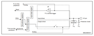
When the I/O port is programmed as analog configuration:
- The output buffer is disabled
- The Schmitt trigger input is deactivated, providing zero consumption for every analog value of the I/O pin. The output of the Schmitt trigger is forced to a constant value (0).
- The weak pull-up and pull-down resistors are disabled by hardware
Read access to the input data register gets the value ‘0’
Address offset:0x00
Reset value: 0xABFF FFFF (for port A)
Reset value: 0xFFFF FEBF (for port B)
Reset value: 0xFFFF FFFF (for port C, D)
Reset value: 0x0000 03FF (for port E)
Reset value: 0x0000 00CF (for port H)
Port E[31:10] are reserved
Port H[31:8, 5:4] are reserved
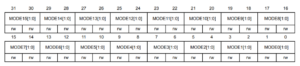
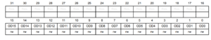
Bits 31:0 MODE[15:0][1:0]: Port x configuration I/O pin y (y = 15 to 0)
These bits are written by software to configure the I/O mode.
00: Input mode
01: General purpose output mode
10: Alternate function mode
11: Analog mode (reset state)
Address offset: 0x04
Reset value: 0x0000 0000
Port E[31:5] are reserved
Port H[31:4, 2] are reserved
Bits 31:16 Reserved, must be kept at reset value.
Bits 15:0 OT[15:0]: Port x configuration I/O pin y (y = 15 to 0)
These bits are written by software to configure the I/O output type.
0: Output push-pull (reset state)
1: Output open-drain
Address offset: 0x08
Reset value: 0x0C00 0000 (for port A)
Reset value: 0x0000 00C0 (for port B)
Reset value: 0x0000 0000 (for other ports)
Bits 31:0 OSPEED[15:0][1:0]: Port x configuration I/O pin y (y = 15 to 0)
These bits are written by software to configure the I/O output speed.
00: Low speed
01: Medium speed
10: Fast speed
11: High speed
Port E[31:10] are reserved
Port H[31:8, 5:4] are reserved
Address offset: 0x0C
Reset value: 0x6400 0000 (for port A)
Reset value: 0x0000 0100 (for port B)
Reset value: 0x0000 0000 (for other ports)
Port E[31:10] are reserved
Port H[31:8, 5:4] are reserved
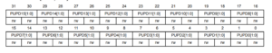
Bits 31:0 PUPD[15:0][1:0]: Port x configuration I/O pin y (y = 15 to 0)
These bits are written by software to configure the I/O pull-up or pull-down
00: No pull-up, pull-down
01: Pull-up 10:
Pull-down
11: Reserved
Address offset: 0x10
Reset value: 0x0000 XXXX
Port E[31:5] are reserved
Port H[31:4, 2] are reserved
Bits 31:16 Reserved, must be kept at reset value.
Bits 15:0 ID[15:0]: Port x input data I/O pin y (y = 15 to 0)
These bits are read-only. They contain the input value of the corresponding I/O port.
Address offset: 0x14
Reset value: 0x0000 0000
Port E[31:5] are reserved
Port H[31:4, 2] are reserved
Bits 31:16 Reserved, must be kept at reset value.
Bits 15:0 OD[15:0]: Port output data I/O pin y (y = 15 to 0)
These bits can be read and written by software.
Address offset: 0x18
Reset value: 0x0000 0000
Port E[31:21, 15:5] are reserved
Port H[31:20, 18, 15:4, 2] are reserved
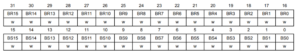
Bits 31:16 BR[15:0]: Port x reset I/O pin y (y = 15 to 0)
These bits are write-only. A read to these bits returns the value 0x0000.
0: No action on the corresponding ODx bit
1: Resets the corresponding ODx bit
Note: If both BSx and BRx are set, BSx has priority.
Bits 15:0 BS[15:0]: Port x set I/O pin y (y = 15 to 0)
These bits are write-only. A read to these bits returns the value 0x0000.
0: No action on the corresponding ODx bit
1: Sets the corresponding ODx bit
Address offset: 0x1C
Reset value: 0x0000 0000
Port E[31:17, 15:5] are reserved
Port H[31:17, 15:4, 2] are reserved
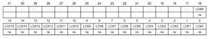
Bits 31:17 Reserved, must be kept at reset value.
Bit 16 LCKK: Lock key This bit can be read any time. It can only be modified using the lock key write sequence.
0: Port configuration lock key not active
1: Port configuration lock key active.
The GPIOx_LCKR register is locked until the next MCU reset or peripheral reset. LOCK key write sequence:
WR LCKR[16] = ‘1’ + LCKR[15:0]
WR LCKR[16] = ‘0’ + LCKR[15:0]
WR LCKR[16] = ‘1’ + LCKR[15:0]
RD LCKR RD LCKR[16] = ‘1’ (this read operation is optional but it confirms that the lock is active)
Note: During the LOCK key write sequence, the value of LCK[15:0] must not change. Any error in the lock sequence aborts the lock.
Bits 15:0 LCK[15:0]: Port x lock I/O pin y (y = 15 to 0)
These bits are read/write but can only be written when the LCKK bit is 0.
0: Port configuration not locked
1: Port configuration locked
Address offset: 0x20
Reset value: 0x0000 0000
Port E[31:20] are reserved
Port H[31:16, 11:8] are reserved

Bits 31:0 AFSEL[7:0][3:0]: Alternate function selection for port x I/O pin y (y = 7 to 0) These bits are written by software to configure alternate function I/Os.
0000: AF0
0001: AF1
0010: AF2
0011: AF3
0100: AF4
0101: AF5
0110: AF6
0111: AF7
1000: AF8
1001: AF9
1010: AF10
1011: AF11
1100: AF12
1101: AF13
1110: AF14
1111: AF15
Address offset: 0x24
Reset value: 0x0000 0000
Port E[31:0] are reserved
Port H[31:0] are reserved
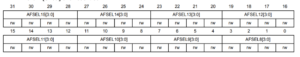
Bits 31:0 AFSEL[15:8][3:0]: Alternate function selection for port x I/O pin y (y = 15 to 8)
These bits are written by software to configure alternate function I/Os.
0000: AF0
0001: AF1
0010: AF2
0011: AF3
0100: AF4
0101: AF5
0110: AF6
0111: AF7
1000: AF8
1001: AF9
1010: AF10
1011: AF11
1100: AF12
1101: AF13
1110: AF14
1111: AF15
Address offset: 0x28
Reset value: 0x0000 0000
Port E[31:5] are reserved
Port H[31:4, 2] are reserved
Bits 31:16 Reserved, must be kept at reset value.
Bits 15:0 BR[15:0]: Port x reset IO pin y (y = 15 to 0)
These bits are write-only. A read to these bits returns the value 0x0000.
0: No action on the corresponding ODx bit
1: Reset the corresponding ODx bit
Refer the Reference Manual for the Complete GPIO Register Map and further information
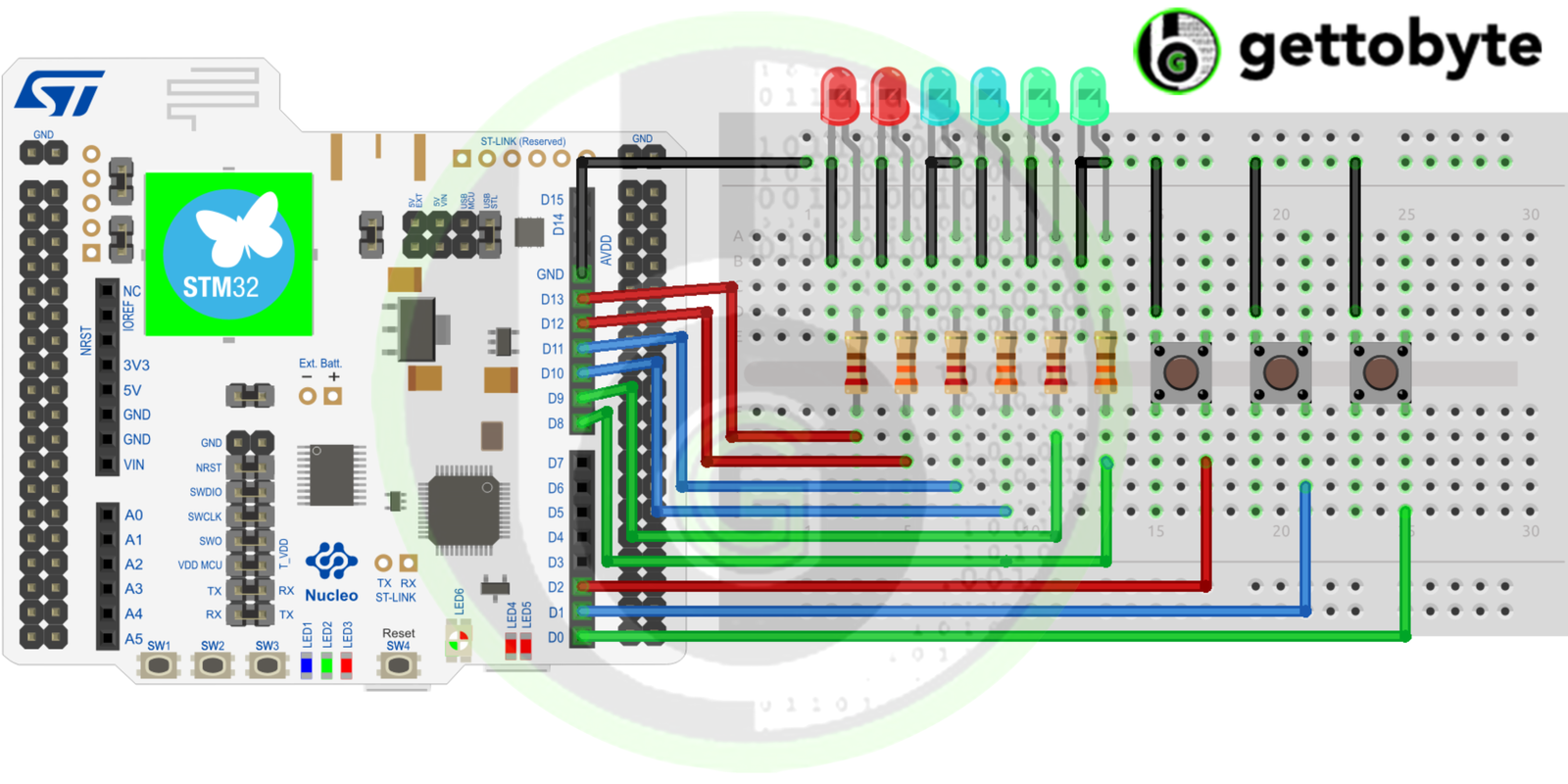
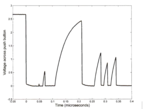
When a mechanical button is PUSHED, two metal contacts bang together and immediately rebounce a couple of times before setting. During this process multiple signals of a few microseconds are produced due to BOUNCE EFFECT, which a processor can easily detect, thus determining the rising and falling transmission and mistakenly thinking that the push button has been pressed multiple times.
There are DEBOUNCING solutions to this bouncing effect which can be done easily by hardware as well as by software.
- HARDWARE DEBOUNCING
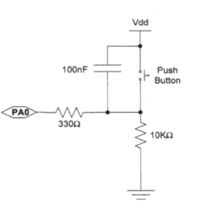
It uses a simple RC circuit, which includes a capacitor connected in parallel with the pushbutton to filter out any high-frequency signals. When the switch is open, this capacitor is fully charged. Therefore, there is no current on these resistors, and the voltage on the processor pin is zero. As soon as the button is pressed, the capacitor is quickly discharged. If the button rebounds and the switch is open briefly, the capacitor cannot be recharged fast enough to pull the processor pin low.
- SOFTWARE DEBOUNCING
Here, the technique is wait-and-see. When the program detects that a button is pressed, it re-examines the input signal after a short delay, typically between 20 and 50 ms. If the input signal still shows the button is pressed, the program then reports that the button has been pressed indeed.
However, the response time of the wait-and-see technique is significant and is not
acceptable in many applications, such as gaming or mission-critical systems. A better software debouncing technique is counter debouncer. It polls the button input at regular intervals and requires a few consecutive positive readings to confirm the button has been pressed.
Here in our example we make the GPIO port Pulled up by default so that when the button is pressed, it’s in the LOW state.
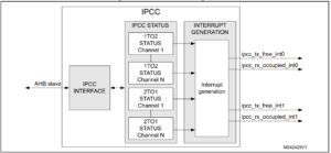
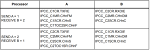
As the name suggest this peripheral ensures the communication between two processors
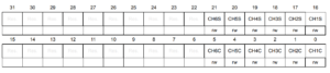
The IPCC block provides a non blocking signaling mechanism to post and retrieve communication data in an atomic way. It provides the signaling for twelve channels:
- 6 channels in the direction from processor 1 to processor 2
- 6 channels in the opposite direction
It is then possible to have two different communication types in each direction. The IPCC communication data must be located in a common memory, which is not part of the IPCC block.
The main features of IPCC are
- Status signaling for the twelve channels
- Channel occupied/free flag, also used as lock
- Two interrupt lines per processor
- One for RX channel occupied (communication data posted by sending processor)
- One for TX channel free (communication data retrieved by receiving processor)
- Interrupt masking per channel
- Channel occupied mask
- Channel free mask
- Two channel operation modes
- Simplex (each channel has its own communication data memory location)
- Half duplex (a single channel associated to a bidirectional communication data information memory location)
Functional Description
The communication data of the IPCC is stored in a shared memory that is separate from the IPCC block. It is necessary to either have knowledge of the address location of the communication data or locate it in a common area that is already known, and this area is distinct from the IPCC block.
For each communication, the IPCC block provides a channel status flag CHnF.
- For Logic Level ‘0’, the flag CHnF indicates that the associated IPCC channel is free (the receiving processor has retrieved communication data), and can be accessed by the sending processor.
- For Logic Level ‘1’, the flag CHnF indicates that the associated IPCC channel is occupied (the sending processor has posted communication data) and can be accessed by the receiving processor.
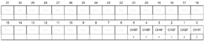
IPCC Simplex Channel Mode
When operating in Simplex channel mode, a specific memory location is allocated for the transfer of data in one direction only. The N control bits related to the channel are utilized to regulate the transfer process from the transmitting processor to the receiving one.
Once the sending processor has posted the communication data in the memory, it sets the channel status flag CHnF to occupied with CHnS.
Once the receiving processor has retrieved the communication data from the memory, it clears the channel status flag CHnF back to free with CHnC.
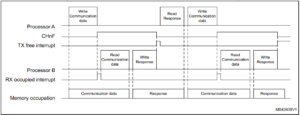
This can be understood easily with the following clock diagram.
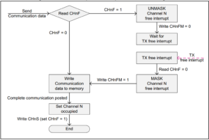
To send communication data:
- The sending processor checks the channel status flag CHnF:
- When CHnF = 0, the channel is free (last communication data retrieved by the receiving processor), and the new communication data can be written.
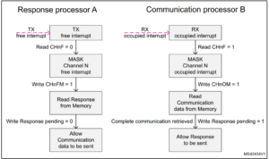
- When CHnF = 1, the channel is occupied (last communication data not retrieved by the receiving processor), and the sending processor unmasks the channel free interrupt (CHnFM = 0).
- On a TX free interrupt, the sending processor checks which channel became free and masks the channel free interrupt (CHnFM = 1). Then the new communication can take place.
- Once the complete communication data is posted, the channel status is set to occupied with CHnS. This gives memory access to the receiving processor and generates the RX occupied interrupt.
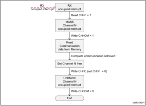
To receive a communication, the channel occupied interrupt is unmasked (CHnOM = 0):
- On an RX occupied interrupt, the receiving processor checks which channel became occupied, masks the associated channel occupied interrupt (CHnOM) and reads the communication data from memory.
- Once the complete communication data is retrieved, the channel status is cleared to free with CHnC. This gives memory access back to the sending processor and may generate the TX free interrupt.
- Once the channel status is cleared, the channel occupied interrupt is unmasked (CHnOM = 0).
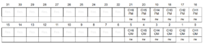
IPCC Half Duplex Channel Mode
The Half-duplex channel mode is used when one processor sends a communication and the other processor sends a response to each communication (ping-pong).
When using Half-duplex channel mode, a solitary memory location is designated for transmitting communication data and receiving responses. This location is utilized for transferring data in both directions. The status flag of the CHnF channel is assigned to the sending processor and is utilized by both processors.
Once the processor A
- Post the communication data into memory.
- Sets Channel Status Flag CHnF for processor A to be occupied with CHnS.
- Thus gives memory access to processor B.
Once the processor B
- Retrieves the data from memory.
- Channel Status Flag CHnF for processor B is unchanged.
- Memory access is kept with processor B for the response.
- After posting response, clears the Channel Status Flag CHnF to free with CHnC.
- Thus it gives memory access back to processor A
After getting the response, the processor A does not change the status of the channel flag for the next communication data.
The timing diagram will give a better idea about the above scenario.
To send communication data:
- The sending processor waits for its response pending software variable to get 0.
- Once the response pending software variable is 0 the communication data is posted.
- Once the complete communication data has been posted, the channel status flag CHnF is set to occupied with CHnS and the response pending software variable is set to 1 (this gives memory access and generates the RX occupied interrupt to the receiving processor).
- Once the channel status flag CHnF is set, the channel free interrupt is unmasked (CHnFM = 0).
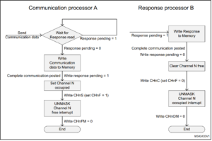
To send a response:
- The receiving processor waits for its response pending software variable to get 1.
- Once the response pending software variable is 1, the response is posted.
- Once the complete response is posted, the channel status flag CHnF is cleared to free with CHnC and the response pending software variable is set to 0 (this gives memory access and generates the TX free interrupt to the sending processor).
- Once the channel status flag CHnF is cleared, the channel occupied interrupt is unmasked (CHnOM = 0).
To receive communication data the channel occupied interrupt is unmasked (CHnOM = 0):
- On a RX occupied interrupt, the receiving processor checks which channel became occupied, masks the associated channel occupied interrupt (CHnOM) and reads the communication data from the memory.
- Once the complete communication data is retrieved, the response pending software variable is set. The channel status is not changed, access to the memory is kept to post the subsequent response.
To receive the response the channel free interrupt is unmasked (CHnFM = 0):
- On a TX free interrupt, the sending processor checks which channel became free, masks the associated channel free interrupt (CHnFM) and reads the response from the memory.
- Once the complete response is retrieved, the response pending software variable is cleared. The channel status is not changed, access to the memory is kept to post the subsequent communication data.
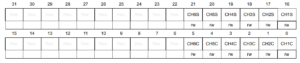
IPCC Interrupts
There are four interrupt lines :
- 2 RX channel occupied interrupts, one for each processor:
- Interrupt enable RXOIE per processor
- Individual mask CHnOM per channel
- 2 TX channel free interrupts, one for each processor
- Interrupt enable TXFIE per processor
- Individual mask CHnFM per channel
The RX occupied interrupt is used by the receiving processor and indicates when an unmasked channel status indicates occupied (CHnF = 1).
The TX free interrupt is used by the sending processor, and indicates when an unmasked channel status indicates free (CHnF = 0).
A secure channel only generates a secure interrupt, and only in the case when the channel is secure unmasked and global secure enabled.
A non-secure channel only generates a non-secure interrupt, and only in the case when the channel is non-secure unmasked and global non-secure enabled.
IPCC_C1CR IPCC Processor 1 Control Register
Address offset: 0x000
Reset value: 0x0000 0000

Bits 31:17 Reserved, must be kept at reset value.
Bit 16 TXFIE: Processor 1 transmit channel free interrupt enable
Associated with IPCC_C1TOC2SR.
1: Enable an unmasked processor 1 transmit channel free to generate a TX free interrupt.
0: Processor 1 TX free interrupt disabled
Bits 15:1 Reserved, must be kept at reset value.
Bit 0 RXOIE: Processor 1 receive channel occupied interrupt enable
Associated with IPCC_C2TOC1SR.
1: Enable an unmasked processor 1 receive channel occupied to generate an RX occupied interrupt.
0: Processor 1 RX occupied interrupt disabled
IPCC_C1MR IPCC Processor 1 Mask Register
Address offset: 0x004
Reset value: 0xFFFF FFFF
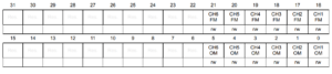
Bits 31:22 Reserved, must be kept at reset value.
Bits 21:16 CHnFM: Processor 1 transmit channel n status set, (n = 6 to 1).
Associated with IPCC_C1TOC2SR.CHnF
1: Transmit channel n free interrupt masked.
0: Transmit channel n free interrupt not masked.
Bits 15:6 Reserved, must be kept at reset value.
Bits 5:0 CHnOM: Processor 1 receives channel n status clear (n = 6 to 1).
Associated with IPCC_C2TOC1SR.CHnF
1: Receive channel n occupied interrupt masked.
0: Receive channel n occupied interrupt not masked.
IPCC_C1SCR IPCC Processor 1 Status Set Clear Register
Address offset: 0x008
Reset value: 0x0000 0000
Reading this register always returns 0x0000 0000.
Bits 31:22 Reserved, must be kept at reset value.
Bits 21:16 CHnS: Processor 1 transmit channel n status set (n = 6 to 1).
Associated with IPCC_C1TOC2SR.CHnF
1: Processor 1 transmit channel n status bit set.
0: No action.
Bits 15:6 Reserved, must be kept at reset value.
Bits 5:0 CHnC: Processor 1 receives channel n status clear (n = 6 to 1).
Associated with IPCC_C2TOC1SR.CHnF
1: Processor 1 receives channel n status bit clear.
0: No action.
IPCC_C1TOC2R IPCC Processor 1 Processor 2 Status Register
Address offset: 0x00C
Reset value: 0x0000 0000
Bits 31:6 Reserved, must be kept at reset value.
Bits 5:0 CHnF: Processor 1 transmit to processor 2 receive channel n status flag before masking (n = 6 to 1).
1: Channel occupied, data can be read by the receiving processor 2.
Generates a channel RX occupied interrupt to processor 2, when unmasked.
0: Channel free, data can be written by the sending processor 1.
Generates a channel TX free interrupt to processor 1, when unmasked.
IPCC_C2CR IPCC Processor 2 Control Register
Address offset: 0x010
Reset value: 0x0000 0000

Bits 31:17 Reserved, must be kept at reset value.
Bit 16 TXFIE: Processor 2 transmit channel free interrupt enable
Associated with IPCC_C2TOC1SR.
1: Enable an unmasked processor 2 transmit channel free to generate a TX free interrupt.
0: Processor 2 TX free interrupt disabled
Bits 15:1 Reserved, must be kept at reset value.
Bit 0 RXOIE: Processor 2 receive channel occupied interrupt enable
Associated with IPCC_C1TOC2SR.
1: Enable an unmasked processor 2 receive channel occupied to generate an RX occupied interrupt.
0: Processor 2 RX occupied interrupt disabled
IPCC_C2MR IPCC Processor 2 Mask Register
Address offset: 0x014
Reset value: 0xFFFF FFFF
Bits 31:22 Reserved, must be kept at reset value.
Bits 21:16 CHnFM: Processor 2 transmit channel n free interrupt mask (n = 6 to 1).
Associated with IPCC_C2TOC1SR.CHnF
1: Transmit channel n free interrupt masked.
0: Transmit channel n free interrupt not masked.
Bits 15:6 Reserved, must be kept at reset value.
Bits 5:0 CHnOM: Processor 2 receives channel n occupied interrupt mask (n = 6 to 1).
Associated with IPCC_C1TOC2SR.CHnF
1: Receive channel n occupied interrupt masked.
0: Receive channel n occupied interrupt not masked.
IPCC_C2SCR IPCC Processor 2 Set Clear Register
Address offset: 0x018
Reset value: 0x0000 0000
Reading this register always returns 0x0000 0000.
Bits 31:22 Reserved, must be kept at reset value.
Bits 21:16 CHnS: Processor 2 transmit channel n status set (n = 6 to 1).
Associated with IPCC_C2TOC1SR.CHnF
1: Processor 2 transmit channel n status bit set.
0: No action.
Bits 15:6 Reserved, must be kept at reset value.
Bits 5:0 CHnC: Processor 2 receives channel n status clear (n = 6 to 1).
Associated with IPCC_C1TOC2SR.CHnF
1: Processor 2 receives channel n status bit clear.
0: No action.
IPCC_C2TOC1R IPCC Processor 2 to Processor 1 Status Register
Address offset: 0x01C
Reset value: 0x0000 0000
Bits 31:6 Reserved, must be kept at reset value.
Bits 5:0 CHnF: Processor 2 transmit to processor 1 receive channel n status flag before masking (n = 6 to 1)
1: Channel occupied, data can be read by the receiving processor 1.
Generates a channel RX occupied interrupt to processor 1, when unmasked.
0: Channel free, data can be written by the sending processor 2.
Generates a channel TX free interrupt to processor 2, when unmasked.
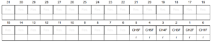
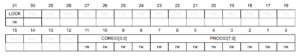
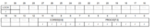
The hardware semaphore block provides 32 (32-bit) register based semaphores.
The semaphores can be used to ensure synchronization between different processes running between different cores. The HSEM provides a non-blocking mechanism to lock semaphores in an atomic way.
The following functions are provided:
- Semaphore lock, in two ways:
- 2-step lock: by writing COREID and PROCID to the semaphore, followed by a read check
- 1-step lock: by reading the COREID from the semaphore
- Interrupt generation when a semaphore is unlocked
- Each semaphore may generate an interrupt on one of the interrupt lines
- Semaphore clear protection
- A semaphore is only unlocked when COREID and PROCID match
- Global semaphore clear per COREID
The HSEM includes the following features:
- 32 (32-bit) semaphores
- 8-bit PROCID
- 4-bit COREID
- One interrupt line per processor
- Lock indication
HSEM Block Diagram and Lock Procedure
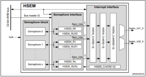
The HSEM is based on three sub-blocks:
- The semaphore block containing the semaphore status and IDs
- The semaphore interface block providing AHB access to the semaphore via the HSEM_Rx and HSEM_RLRx registers
- The interrupt interface block provides control for the interrupts via HSEM_CnISR, HSEM_CnIER, HSEM_CnMISR, and HSEM_CnICR registers.
If LOCK Bit is ‘0’
- Semaphore is considered FREE
- COREID and PROCID are also ‘0’
If LOCK bit ‘1’
- Semaphore is locked.
- COREID indicated which of the AHB bus master is locked
- PROCID indicated which process of that AHB bus master ID has been locked.
Writing Locking,
- COREID must match the AHB bus master ID
- PROCID written by AHB bus master software process taking the lock
Reading Locking
- COREID is taken from the AHB bus master ID
- PROCID is forced by hardware to be ‘0’. Thus no PROCID is available with read lock
2-step (write) lock procedure
The 2-step lock procedure consists in a write to lock the semaphore, followed by a read to check if the lock has been successful, carried out from the HSEM_Rx register.
- Write semaphore with PROCID and COREID, and LOCK = 1. The COREID data written by software must match the AHB bus master information, that is, a AHB bus master ID = 1writes data COREID = 1.
Lock is put in place when the semaphore is free at write time.
- Read-back the semaphore The software checks the lock status, if PROCID and COREID match the written data, then the lock is confirmed.
- Else retry (the semaphore has been locked by another process, AHB bus master ID).
A semaphore can only be locked when it is free.
A semaphore can be locked when the PROCID = 0.
Consecutive write attempts with LOCK = 1 to a locked semaphore are ignored.
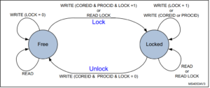
1-step (read) lock procedure
The 1-step procedure consists in a read to lock and check the semaphore in a single step, carried out from the HSEM_RLRx register.
- Read lock semaphore with the AHB bus master COREID.
- If read COREID matches and PROCID = 0, then lock is put in place.
- If COREID matches and PROCID is not 0, this means that another process from the same COREID has locked the semaphore with a 2-step (write) procedure.
- Else retry (the semaphore has been locked by another process, AHB bus master ID).
When read locking a free semaphore, PROCID is 0.
Read locking a locked semaphore returns the COREID and PROCID that locked it.
All read locks, including the first one that locks the semaphore, return the COREID that locks or locked the semaphore
HSEM Write/Read/Read Lock Register Address
For each semaphore, two AHB register addresses are provided, separated in two banks of 32-bit semaphore registers, spaced by a 0x80 address offset.
In the first register address bank the semaphore can be written (locked/unlocked) and read through the HSEM_Rx registers.
In the second register address bank the semaphore can be read (locked) through the HSEM_RLRx registers.
HSEM Unlock Procedures
To avoid any unintentional clearing of a semaphore by an unauthorized AHB bus master ID or process, unlocking a semaphore is a secure process. To unlock the semaphore, one must write to the semaphore’s HSEM_Rx register with the corresponding COREID and PROCID while setting LOCK to 0. When successfully unlocked, both the COREID and PROCID will be set to 0.
When unlocked, an interrupt may be generated to signal the event. To this end, the semaphore interrupt must be enabled.
The unlock procedure consists in a write to the semaphore HSEM_Rx register with matching COREID regardless of how the semaphore has been locked (1- or 2-step).
- Write semaphore with PROCID, COREID, and LOCK = 0
- If the written data matches the semaphore PROCID and COREID and the AHB bus master ID , the semaphore is unlocked and an interrupt may be generated when enabled, else write is ignored, semaphore remains locked and no interrupt is generated (the semaphore is locked by another process, AHB bus master ID or the written data does not match the AHB bus master signaling).
Note: Different processes of the same AHB bus master ID can write any PROCID value. Preventing other processes of the same AHB bus master ID from unlocking a semaphore must be ensured by software, handling the PROCID correctly
HSE COREID Semaphore Clear
It is possible to unlock all semaphores that have been locked by a specific COREID at once by utilizing the HSEM_CR register. To unlock these semaphores, one must write the corresponding COREID and the correct KEY value in the HSEM_CR register. All semaphores that are locked by a matching COREID will be unlocked as a result, and it may trigger an interrupt if it has been enabled.
An interrupt may be generated for the unlocked semaphore(s). To this end, the semaphore interrupt must be enabled in the HSEM_CnIER registers.
HSEM Interrupts
An interrupt line hsem_intn_it per processor allows each semaphore to generate an interrupt.
An interrupt line provides the following features per semaphore:
- interrupt enable
- interrupt clear
- interrupt status
- masked interrupt status
With the interrupt enable (HSEM_CnIER) the semaphores affecting the interrupt line can be enabled. Disabled (masked) semaphore interrupts do not set the masked interrupt status MISF for that semaphore, and do not generate an interrupt on the interrupt line. The interrupt clear (HSEM_CnICR) clears the interrupt status ISF and masked interrupt status MISF of the associated semaphore for the interrupt line.
The interrupt status (HSEM_CnISR) mirrors the semaphore interrupt status ISF before the enable.
The masked interrupt status (HSEM_CnMISR) only mirrors the semaphore enabled interrupt status MISF on the interrupt line. All masked interrupt status MISF of the enabled semaphores need to be cleared to clear the interrupt line.
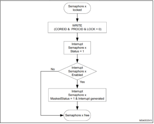
Try to lock semaphore x
- If the semaphore lock is obtained, no interrupt is needed.
- If the semaphore lock fails:
- Clear pending semaphore x interrupt status for the interrupt line in HSEM_CnICR. Re-try to lock the semaphore x again:
- If the semaphore lock is obtained, no interrupt is needed (semaphore has been freed between first try to lock and clear semaphore interrupt status).
- If the semaphore lock fails, enable the semaphore x interrupt in HSEM_CnIER.
On semaphore x free interrupt, try to lock semaphore x
- If the semaphore lock is obtained:
Disable the semaphore x interrupt in HSEM_CnIER.
Clear pending semaphore x interrupt status in HSEM_CnICR.
- If the semaphore x lock fails:
Clear pending semaphore x interrupt status in HSEM_CnICR.
Try again to lock the semaphore x:
- If the semaphore lock is obtained (semaphore has been freed between first try to lock and semaphore interrupt status clear), disable the semaphore interrupt in HSEM_CnIER.
- If the semaphore lock fails, wait for a semaphore free interrupt.
AHB Bus Master ID Verification
The HSEM allows only authorized AHB bus master IDs to lock and unlock semaphores.
- The AHB bus master 2-step lock write access to the semaphore HSEM_Rx register is checked against the valid bus master IDs.
- Accesses from unauthorized AHB bus master IDs are discarded and do not lock the semaphore.
- The AHB bus master 1-step lock read access from the semaphore HSEM_RLRx register is checked against the valid bus master IDs.
- An unauthorized AHB bus master ID read from HSEM_RLRx returns all 0.
- The semaphore unlock write access to the HSEM_CR register is checked against the valid bus master IDs. Only the valid bus master IDs can write to the HSEM_CR register and unlock any of the COREID semaphores.
- Accesses from unauthorized AHB bus master IDs are discarded and do not clear the COREID semaphores.
![]()
HSEM_Rx HSEM Register Semaphore
Address offset: 0x000 + 0x4 * x (x = 0 to 31)
Reset value: 0x0000 0000
The HSEM_Rx must be used to perform a 2-step write lock, read back, and for unlocking a semaphore. Only write accesses with authorized AHB bus master IDs are granted. Write accesses with unauthorized AHB bus master IDs are discarded.
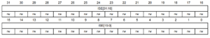
Bit 31 LOCK: Lock indication
This bit can be written and read by software.
0: On write free semaphore (only when COREID and PROCID match), on read semaphore is free.
1: On write try to lock semaphore, on read semaphore is locked.
Bits 30:13 Reserved, must be kept at reset value.
Bit 12 Reserved, must be kept at reset value.
Bits 11:8 COREID[3:0]: Semaphore COREID
Written by software
- When the semaphore is free and the LOCK bit is at the same time written to 1 and the COREID matches the AHB bus master ID.
- When the semaphore is unlocked (LOCK written to 0 and AHB bus master ID matched COREID, the COREID is cleared to 0.
- When the semaphore is unlocked (LOCK bit written to 0 or AHB bus master ID does not match COREID, the COREID is not affected.
- Write when LOCK bit is already 1 (semaphore locked), the COREID is not affected.
- An authorized read returns the stored COREID value.
Bits 7:0 PROCID[7:0]: Semaphore PROCID
Written by software
- When the semaphore is free and the LOCK is written to 1, and the COREID matches the AHB bus master ID, PROCID is set to the written data.
- When the semaphore is unlocked, LOCK written to 0 and AHB bus master ID matched COREID, the PROCID is cleared to 0.
- When the semaphore is unlocked, LOCK bit written to 0 and AHB bus master ID does not match COREID, the PROCID is not affected.
- Write when LOCK bit is already 1 (semaphore locked), the PROCID is not affected.
- An authorized read returns the stored PROCID value.
HSEM_RLRx HSE Read Lock Register Semaphore
Address offset: 0x080 + 0x4 * x (x = 0 to 31)
Reset value: 0x0000 0000
Accesses the same physical bits as HSEM_Rx. The HSEM_RLRx must be used to perform a 1-step read lock. Only read accesses with authorized AHB bus master IDs are granted. Read accesses with unauthorized AHB bus master IDs are discarded and return 0.
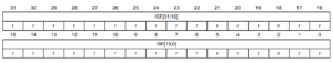
Bit 31 LOCK: Lock indication
This bit is read only by software at this address.
- When the semaphore is free: A read with a valid AHB bus master ID locks the semaphore and returns 1.
- When the semaphore is locked: A read with a valid AHB bus master ID returns 1 (the COREID and PROCID reflect the already locked semaphore information).
Bits 30:13 Reserved, must be kept at reset value.
Bit 12 Reserved, must be kept at reset value.
Bits 11:8 COREID[3:0]: Semaphore COREID
This field is read only by software at this address.
On a read, when the semaphore is free, the hardware sets the COREID to the AHB bus master ID reading the semaphore. The COREID of the AHB bus master locking the semaphore is read.
On a read when the semaphore is locked, this field returns the COREID of the AHB bus master that has locked the semaphore.
Bits 7:0 PROCID[7:0]: Semaphore processor ID
This field is read only by software at this address.
- On a read when the semaphore is free: A read with a valid AHB bus master ID locks the semaphore and hardware sets the PROCID to 0.
- When the semaphore is locked: A read with a valid AHB bus master ID returns the PROCID of the AHB bus master that has locked the semaphore.
HSEM_CnIER HSEM Interrupt Enable Register
Address offset: 0x100 + 0x010 * (n – 1), (n = 1 to 2)
Reset value: 0x0000 0000
Bits 31:0 ISE[31:0]: Interrupt(n) semaphore x enable bit (x = 0 to 31)
This bit is read and written by software.
0: Interrupt(n) generation for semaphore x disabled (masked)
1: Interrupt(n) generation for semaphore x enabled (not masked)
HSEM_CnICR HSEM Interrupt Clear Register
Address offset: 0x104 + 0x010 * (n – 1), (n = 1 to 2)
Reset value: 0x0000 0000

Bits 31:0 ISC[31:0]: Interrupt(n) semaphore x clear bit (x = 0 to 31)
This bit is written by software, and is always read 0.
0: Interrupt(n) semaphore x status ISFx and masked status MISFx not affected.
1: Interrupt(n) semaphore x status ISFx and masked status MISFx cleared.
HSEM_CnISR HSEM Interrupt Status Register
Address offset: 0x108 + 0x010 * (n – 1), (n = 1 to 2)
Reset value: 0x0000 0000
Bits 31:0 ISF[31:0]: Interrupt semaphore x status bit before enable (mask) (x = 0 to 31)
This bit is set by hardware, and reset only by software. This bit is cleared by software writing the corresponding HSEM_CnICR bit.
0: Interrupt semaphore x status, no interrupt pending
1: Interrupt semaphore x status, interrupt pending
HSEM_MISR HSEM Interrupt Status Register
Address offset: 0x10C + 0x010 * (n – 1), (n = 1 to 2)
Reset value: 0x0000 0000

Bits 31:0 MISF[31:0]: Masked interrupt(n) semaphore x status bit after enable (mask) (x = 0 to 31)
This bit is set by hardware and read only by software. This bit is cleared by software writing the corresponding HSEM_CnICR bit. This bit is read as 0 when semaphore x status is masked in HSEM_CnIER bit x.
0: interrupt(n) semaphore x status after masking not pending
1: interrupt(n) semaphore x status after masking pending
HSEM_CR HSEM Clear Register
Address offset: 0x140
Reset value: 0x0000 0000
Only write accesses with authorized AHB bus master IDs are granted. Write accesses with unauthorized AHB bus master IDs are discarded.
Bits 31:16 KEY[15:0]: Semaphore clear key
This field can be written by software and is always read 0. If this key value does not match HSEM_KEYR.KEY, semaphores are not affected. If this key value matches HSEM_KEYR.KEY, all semaphores matching the COREID are cleared to the free state.
Bits 15:13 Reserved, must be kept at reset value.
Bit 12 Reserved, must be kept at reset value.
Bits 11:8 COREID[3:0]: COREID of semaphores to be cleared
This field can be written by software and is always read 0.
This field indicates the COREID for which the semaphores are cleared when writing the HSEM_CR.
Bits 7:0 Reserved, must be kept at reset value.
HSEM_KEYR HSEM Clear Semaphore Key Register
Address offset: 0x144
Reset value: 0x0000 0000
Bits 31:16 KEY[15:0]: Semaphore clear key
This field can be written and read by software. Key value to match when clearing semaphores.
Bits 15:0 Reserved, must be kept at reset value.