

Figure 2: Pull-up and Pull-Down Configuration
This configuration consist of a pair of complementary transistors which works as:
- For LOGIC 0, the transistor connected to the ground is turned on to sink an electric current from the external circuit.
- For LOGIC 1, the transistor connected to the power supply is turned on, and it provides an electric current to the external circuit connected to the output pin.
The slave address of the MPU-6050 id 0b110100x, a 7-bit long. Here the LSB bit i.e.x in the 7-bit long address is determined by the logic level at AD0 pin.If x=0 i.e., pin AD0 is Logic LOW otherwise Logic HIGH.

Figure 3: Push-Pull Configuration


Figure 4: The Logic 0 and 1 for Push-Pull Configuration
This configuration consist of a single transistors which works as:
- For LOGIC 0, the transistor connected to the ground is turned on to sink an electric current from the external circuit.
- For LOGIC 1, it cannot supply any electric current to the external load because the output pin is floating, connected to neither the power supply nor the ground.
Hence the Open-Drain has two states LOGIC 0 (LOW) and LOGIC 1 (Z-STATE). This configuration use external pull up resistor.

Figure 5: Open-Drain Configuration

Figure 6: The Logic 0 and 1 for Open-Drain Configuration

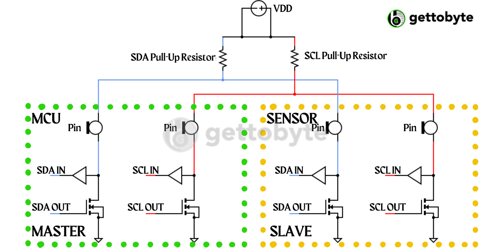
Figure 7: I2C Block Diagram
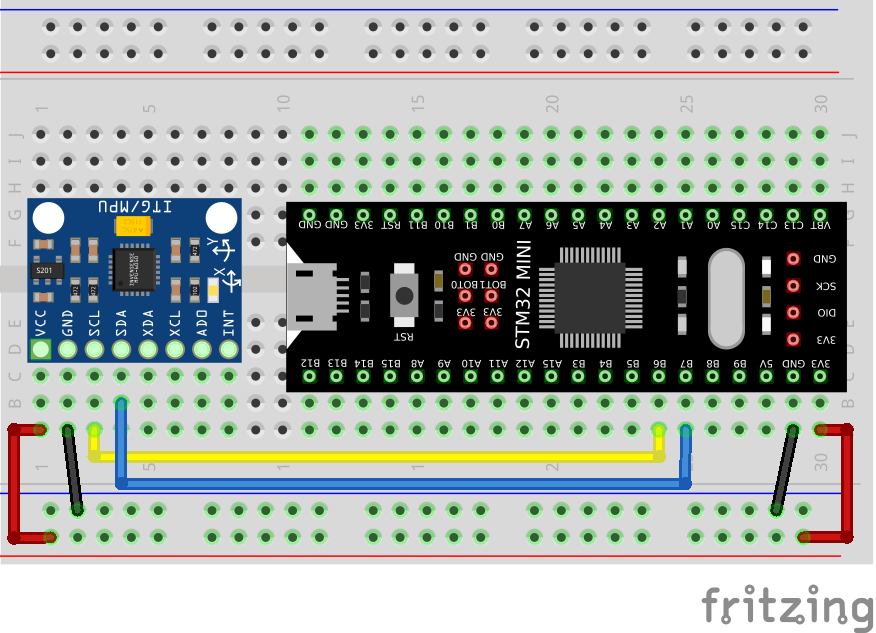
Set up the RCC ad the SYS in the STM32Cube IDE as shown:
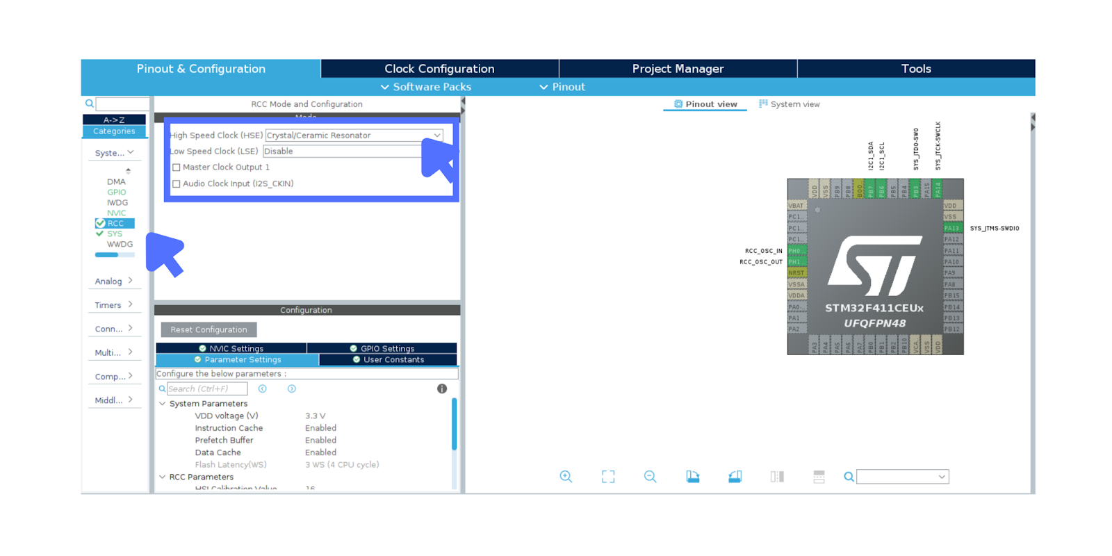

Now enable the I2C1 in the standard mode.

Below is the algorithm for MPU_Init().
Firstly, we will verify the device by checking the presence of the sensor with REG_WHO_AM_I (0x75) using HAL_I2C_Mem_Write ()

HAL_I2C_Mem_Write () function has the following parameters:
-
hi2c: Pointer to a I2C_HandleTypeDef structure that contains the configuration information for the specified I2C.
-
DevAddress: Target device address: The device 7 bits address value in datasheet must be shifted to the left before calling the interface
-
MemAddress: Internal memory address
-
MemAddSize: Size of internal memory address
-
pData: Pointer to data buffer
-
Size: Amount of data to be sent
-
Timeout: Timeout duration
In this case the sensor should return 0x68.
If the sensor successfully returns 0x68, then we need to wake up the sensor which is done by REG_PWR_MGMT_1 (0x6B) register by writing 0x00 to it. The clock is set up to 8MHz.


Next we will set the Data Output rate or simply the Sampling Rate for the data and for that we will use the REG_SMPLRT_DIV (0x19) register. We have set the sampling rate to 1KHz.

As shown in the formula, where the Gyroscope Output Rate is 8KHz so to make Sample Rate = 1KHz, SMPLRT_DIV should be equal to 7.
Further, configure the Full Scale range of Accelerometer and Gyroscope for REG_GYRO_CONFIG (0x1B) and REG_ACCEL_CONFIG (0x1C) registers by writing 0x00.
The REG_ACCEL_CONFIG are XA_ST=0,YA_ST=0,ZA_ST=0, FS_SEL=0 -> ± 2g.


Similarly, REG_GYRO_CONFIG are XG_ST=0,YG_ST=0,ZG_ST=0, FS_SEL=0 -> ± 250 °/s


The code for the same is as follows:
void MPU_Init(void)
{
Uint8_t Check;
uint8_t Data;
HAL_I2C_Mem_Read (&hi2c1, MPU6050_ADDR, REG_WHO_AM_I, 1, &Check, 1, 1000);
if (Check == 0x68)
{
Data = 0;
HAL_I2C_Mem_Write(&hi2c1, MPU6050_ADDR, REG_PWR_MGMT_1, 1,&Data, 1, 1000);
Data = 0x07;
HAL_I2C_Mem_Write(&hi2c1, MPU6050_ADDR, REG_SMPLRT_DIV, 1, &Data, 1, 1000);
Data = 0x00;
HAL_I2C_Mem_Write(&hi2c1, MPU6050_ADDR, REG_ACCEL_CONFIG, 1, &Data, 1, 1000);
Data = 0x00;
HAL_I2C_Mem_Write(&hi2c1, MPU6050_ADDR, REG_GYRO_CONFIG, 1, &Data, 1, 1000);
}
}
With this we are code with the initialization of the module. Next we move to read the values of Accelerometer and Gyroscope.
Below is the algorithm for MPU_Accel_Read():
Firstly let’s discuss the HAL_I2C_Mem_Read(). It has the following parameters:
- hi2c: Pointer to a I2C_HandleTypeDef structure that contains the configuration information for the specified I2C.
- DevAddress: Target device address: The device 7 bits address value in datasheet must be shifted to the left before calling the interface
- MemAddress: Internal memory address
- MemAddSize: Size of internal memory address
- pData: Pointer to data buffer
- Size: Amount of data to be sent
- Timeout: Timeout duration
Here we will use REG_ACCEL_XOUT_H (0x3B – 0x40).


Here it is clearly being observed that it is a 16 bit data being stored as [15:8] and [7:0] in the HIGHER and LOWER ACCEL_XOUT respectively.
Hence we need a 6 bytes array to store the lower and higher values of X, Y, Z axis respectively.
Also we will be doing a bitwise left shift operation along with bit wise OR to get the 16 bit RAW data.
For example ACCEL_XOUT_H is 11000110 and ACCEL_XOUT_L is 00101110 then ACCEL_XOUT will be (11001110 << 8 | 00101110) = 1100111000101110 a 16 bit RAW value.
Why I am constantly saying this is a RAW value is because you can see in the diagram that for a Full-Scale ‘2g’ the sensitivity is 16834 LSB/g. So to get the actual value we need to divide this RAW value by 16384.
The code for the same is as follows:
void MPU_Accel_Read_(MPU6050_ACCEL_t *Mpu_Accel)
{
uint8_t Read_Data[6];
HAL_I2C_Mem_Read (&hi2c1, MPU6050_ADDR, REG_ACCEL_XOUT_H, 1, Read_Data, 6, 1000);
int16_t Accel_X_RAW = (int16_t)(Rec_Data[0] << 8 | Read_Data [1]);
int16_t Accel_Y_RAW = (int16_t)(Rec_Data[2] << 8 | Read_Data [3]);
int16_t Accel_Z_RAW = (int16_t)(Rec_Data[4] << 8 | Read_Data [5]);
Mpu_Accel -> Accel_X = (Accel_X_RAW)/16384.0;
Mpu_Accel -> Accel_Y = (Accel_Y_RAW)/16384.0;
Mpu_Accel -> Accel_Z = (Accel_Z_RAW)/16384.0;
}
Similar is the case for Gyroscope Readings.
Below is the algorithm for the same.
Here we will use REG_GYRO_XOUT_H (0x43 – 0x48).


Here it is clearly being observed that it is a 16 bit data being stored as [15:8] and [7:0] in the HIGHER and LOWER GYRO_XOUT respectively.
Hence we need a 6 bytes array to store the lower and higher values of X, Y, Z axis respectively.
Also we will be doing a bitwise left shift operation along with bit wise OR to get the 16 bit RAW data.
Lastly, the RAW value for a Full-Scale ‘250 dps’ sensitivity is131 LSB/dps. So to get the actual value we need to divide this RAW value by 131..
The code is as follows:
void MPU_Gyro_Read (MPU6050_GYRO_t *Mpu_Gyro)
{
uint8_t Read_Data[6];
HAL_I2C_Mem_Read (&hi2c1, MPU6050_ADDR, REG_GYRO_XOUT_H, 1, Read_Data, 6, 1000);
int16_t Gyro_X_RAW = (int16_t)(Rec_Data[0] << 8 | Read_Data [1]);
int16_t Gyro_Y_RAW = (int16_t)(Rec_Data[2] << 8 | Read_Data [3]);
int16_t Gyro_Z_RAW = (int16_t)(Rec_Data[4] << 8 | Read_Data [5]);
Mpu_Gyro -> Gyro_X = (Gyro_X_RAW)/131.0;
Mpu_Gyro -> Gyro_Y = (Gyro_Y_RAW)/131.0;
Mpu_Gyro -> Gyro_Z = (Gyro_Z_RAW)/131.0;
}
