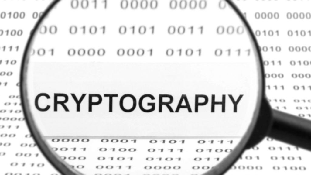
Altium designer is a PCB schematic design and layout tool, which is used to make component libraries and custom footprints, when they are not available from the manufacturer or the suppliers website. Altium even lets the user import custom made CAD files of the component, which can later be simulated to conduct thermal, electrical and RF tests. Altium Designer even has a built in SPICE simulation tool which rivals stand alone softwares in the same class. This SPICE simulation is used to conduct stability, power dissipation, impedance matching and power transfer analysis of the circuit which will be laid out later. This lets the design team save considerable money when developmental tests cannot be performed on these circuits. Altium designer is good not only because it gives the designer tools to help his PCB design process easier but it also comes with built in solutions which include videos, documentation and webinars, which pop-up and are available on the home page when the user enters. Altium design software requires a licence to operate and can be bought for a monthly fee of 20,250 rupees or a perpetually for rupees 600,000.
What is Altium? Altium is a PCB design tool, PCB stands for Printed Circuit Boards and the designing process for a PCB include: Schematic capture, Layout, SPICE simulations, Library and footprint creation, Part tracking, sourcing and revision tracking of both the components used in the design and design itself. It is like git for PCBs and Altium provides tools and resources for all parts of the PCB design workflow.The Altium designer comes with an easy-to-use interface that has lots of features for the PCB designer, like revision control and hot-keys. Altium has 4 SoftwareAltium DesignerAltium NexusAltium Circuit StudioAltium Circuit Maker Previous Next All these software provide a robust framework for the PCB designer to acquire skills of a cross-function multidisciplinary role, because PCB design requires understanding and knowledge of electronic, electrical, and mechanical theory and implementation mechanisms like testing equipment used, designing equipment, and of course manufacturing. Altium software offers the user the ability to interact and collaborate with the mechanical, electronic, and electrical designer through various tools integrated into the software which provide a seamless and robust framework for the designer. Figure 1 Altium 3D mechanical rendering. With the increase in remote working Altium software also offer cloud storage for saving projects, rendering projects, and even saving and running SPICE simulations!
Explore this blog to explore basics of UART Communication protocol in Semiconductor Chip world
Why do we need a rectifier Circuit? Whenever DC power is needed that time, we need to convert an AC Power to DC Power and that process is known as Rectification. A simple PN junction diode acts as a rectifier. The forward biassing and reverse biassing conditions of the diode makes the rectification. Types of Rectifier circuits There are two main types of rectifier circuits, depending upon their output. They are Half-wave Rectifier Full-wave Rectifier A Half-wave rectifier circuit rectifies only positive half cycles of the input supply whereas a Full-wave rectifier circuit rectifies both positive and negative half cycles of the input supply. Half-wave Rectifier Disadvantages of a half-wave rectifier Power is delivered only during the one-half cycle of the input alternating voltage. Ripple factor is high, therefore required to give steady dc output. They only allow a half cycle through per sine wave, and the other half cycle is wasted. This leads to power loss. Full-wave rectifier FWR has two types as follows: Centre tapped full wave rectifier Bridge full-wave Rectifier 1) Centre tapped full wave rectifier Advantages of a center-tapped full-wave rectifier: The ripple factor is much less than that of a half-wave rectifier. DC load current values are twice those of a half-wave rectifier. The rectification efficiency of the full-wave rectifier is double that of a half-wave rectifier. Disadvantages of center-tapped full-wave rectifier Location of center-tapping is difficult. The dc output voltage is small. The PIV of the diodes should be high. 2) Full-wave bridge rectifier Advantages of bridge rectifier: The need for the center-tapped transformer is eliminated. It can be used in application floating output terminals; no output terminal is grounded. The transformer utilization factor, in the case of the bridge rectifier, is higher than that of a center tap rectifier. Disadvantages of Bridge Rectifiers over center tap rectifiers. It requires four diodes for operation, thus, circuit components requirements in the case of the bridge rectifier are more than that of center tap rectifiers. The voltage drop across diodes increases four times that of a center tap full-wave rectifier. Types of Components and Its Symbol used in circuit Schematic of bridge rectifier PCB Layout of bridge rectifier Track Width – 1.00 mm Bill of material During the PCB assembly process, a BOM provides information about the components under a single roof such as their quantity, reference designators, footprints, etc. Designers will save lots of time and effort during PCB design by preparing a bill of materials with all the updated parts list. Every line of the bill of materials (BOM) includes the product code, part name, part number, part revision, description, quantity, unit of measure, size, length, weight, and specifications or features of the product. Go to fabrication bar in Easyeda online tool Download BOM Gerber File Each artwork layer, copper circuitry, power, or ground must have a corresponding Gerber file to create the required pattern. The outermost layers, referenced as “top” and “bottom,” component and solder or by layer count will also have a conforming layer for solder mask and silkscreen to be applied. Summary In this second blog, we have created a schematic of bridge rectifier and pcb layout also and learnt about bill of material and Gerber file. Apart from that we have seen that type of rectifier and understood which one is suitable for industry. Reference https://www.powerelectronicsnews.com/power-supply-design-notes-rectifier-circuits/ https://www.tutorialspoint.com/electronic_circuits/electronic_circuits_full_wave_rectifier.htm https://www.allaboutcircuits.com/textbook/semiconductors/chpt-3/rectifier-circuits/
Static is a keyword in the c/cpp language. It is a storage class specifier that can be applied to any data type. A static keyword can be used with both variables and functions. The static keyword tells the compiler to make the variable or function limited to scope but allows it to persist throughout the life of a program. The static keyword limits the scope of variables or functions to the current source file only. So static keyword helps in hiding the data to one source file only. Static words help in achieving encapsulation in c language. In this blog, we are going to cover the use of static keywords with variables. Static variables are stored in BSS or data segment of the C program Memory Layout. The BSS segment contains the uninitialized data. The DATA segment keeps the initialized data. The static variable is only initialized once, if it is not initialized then it is automatically initialized to 0. void demo(int value) { static int count = 0; count = value; cout<<count; } count = value: is not initialization, it is an assignment. Static can be assigned as many times as we wish. static int count = 0: is initialization & that happens only once for static variables. We can have static global variables or static local variables. Static local variables Static variables are able to retain their value b/w function calls. Static keywords, when used with variables inside the function, are then called static local variables. Static global variables The static keywords when used with variables outside the functions, are then called static global variables. Static global variables help in achieving enumeration, that is they make the scope of the variable limited to the present file only. References: The static keyword in C (c-programming-simple-steps.com)
Here we will understand the basic terms related to microcontrollers.
Explore this blog to explore basics of SPI Communication protocol in Semiconductor Chip world
Hello Friends, This is the second blog of the series of PCB designing. Today we are discussing Steps for PCB Designing, Types of Component and methods for mounting components onto a PCB and designing steps. So before discussing the Method for Mounting Components on PCB, first we will discuss the process or different stages of PCB designing. In order to design a PCB, one has to follow below steps : 1. Create the schematic 2. Link footprints to the components in the schematic 3. Generate a netlist 4. Create desired PCB shape in PCB editor 5. Import the netlist in PCB editor 6. Define design rules 7. Place the footprint of the component at desired location 8. Route the tracks to form electrical connections between various components 9. Add labels and identifiers on PCB 10. Generate design file Types of Components and Its Symbol :- So these are some symbols that are used to prepare the schematic. Methods for mounting components onto a PCB. 1. Through Hole: Through-hole components are best used for high-reliability products that require stronger connections between layers. Through-hole component leads run through the board, allowing the components to withstand more environmental stress. This is why through-hole technology is commonly used in military, automobile, and aerospace products that may experience extreme accelerations, collisions, or high temperatures. Through-hole technology is also useful in test and prototyping applications that sometimes require manual adjustment and replacement. 2. SMD (surface-mount devices): SMD components are much smaller than THM components. This will increase the overall density of the board tremendously. Using a Pick and Place machine for placing the components will reduce production time.SMD components are mostly cheaper compared to THM components. surface-mount devices (SMDs) are secured only by solder on the surface of the board SMD components are not suitable for prototyping or testing of small circuits. SMDs cannot be used directly with breadboards SMD solder connections may be damaged by potting compounds going through thermal cycling. EasyEDA Online Tool We will start from EasyEDA, a great web-based EDA(Electronics Design Automation) tool for electronics engineers, educators, students, makers, and enthusiasts. There is no need to install any software. Just open EasyEDA in Browser. EasyEDA Provides: Simple, Easy, Friendly, and Powerful drawing capabilities Works Anywhere, Anytime, on Any Device Real-time Team Cooperation Sharing Online Thousands of open-source projects Integrated PCB fabrication and Components purchase workflow API provided Script support Schematic Capture PCB Layout: Design Rules Checking(DRC) Multi-Layer, 6 copper layer supported Document export(PDF, PNG, SVG) Altium Designer format export BOM export 3D View Generate fabrication file(Gerber) Export Pick and Place file Auto Router Designing Steps Open EasyEDA Tool On Browser Register in EasyEDA Create New Project Draw Schematic Convert that file into BoARD FILE Track the air wire Select needed layers Print the Document Summary In this second blog, we introduced designing steps. Then we discussed the method of mounting components. Introduced the Easyeda Online tool. Reference : https://payatu.com/blog/rupesh/PCB%20Designing%20-%20Basics https://blog.thedigisource.com/through-hole-smt https://www.vishay.com/docs/45242/throughholevssmdcomponents.pdf https://eprpartner.com/through-hole-vs-surface-mounted https://docs.easyeda.com/en/Introduction/Introduction-to-EasyEDA/index.html https://circuitdigest.com/article/design-electronic-circuits-online-with-easyeda
Here we will understand the basic terms related to microcontrollers.
Compiled language: are translated to the target machine\’s native language by a program called a compiler. This can result in very fast code, especially if the compiler is effective at optimizing however the resulting code may not port well across the operating system & the compilation process may take a while e.g C or CPP. Interpreted Language: is read by a program called an interpreter & is executed by that program called an interpreter and is executed by that program. While they are portable as their interpreter & have no long compile times. e.g Python & Java. High-Level Programming: Refers to how much the nature of language reflects the understanding system. In other words, a programming language level refers to how similar the language is to a computer\’s native language. Low-Level language is generally quite similar to machine code & thus is more suitable for programs like device drivers or very high-performance programs that really need access to hardware. Since a low-level language is subject to all the nuances of the hardware it\’s accessing. Supported Paradigm: