
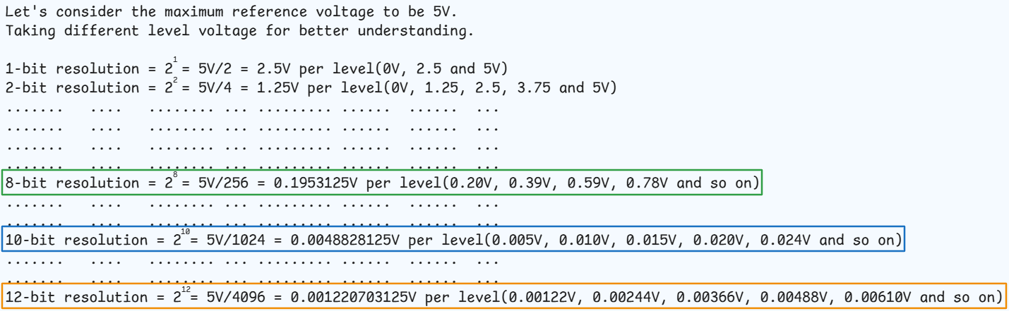
> Single-ended 12-bit, 10-bit, and 8-bit Output Modes
- ADC counter is basically ADC data result register where ADC readings are stored. For Each ADC pin, there is one ADC Data result register: (RA-RP).
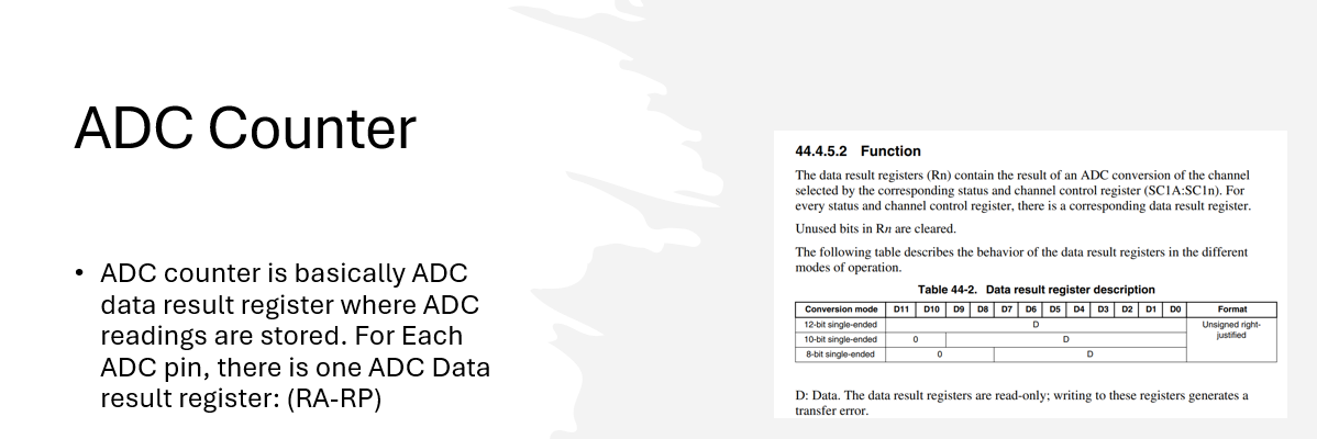
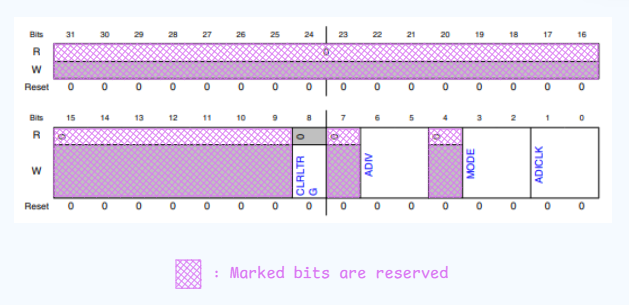
- ADC counter value is selected via MODE bits of ADC CFG1 register.

ADC Data Result Register - These output modes resemble the Resolution of ADC.
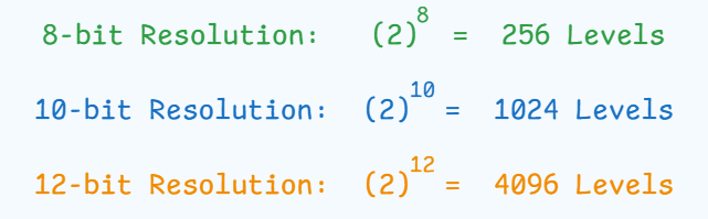
- Let’s break down how precision increases with an increase in resolution. 8-bit resembles that 2 raise to the power 8 = 256 which means only in 256 distinct levels an analog signal can be sliced. Similarly for 10-bit resolution, 10-bit resembles that 2 raise to the power 10 = 1024 which means only in 1024 distinct levels an analog signal can be sliced. Also same goes for 12-bit resolution, the number of distinct levels is 4096 = 2 raising to the power 12.
- Let’s say that we are taking reference of 5V for ADC conversion, reference creates a band of operating range where an Amplitude of 5V is the maximum analog input that can converted by ADC and an amplitude greater than 5V will only show the maximum reference value. You can change the reference for the ADC as per the microcontroller specification mentioned in the datasheet.
- Coming back to our 5V reference, now for this reference we can also calculate the precision level of resolution. if we choose 8-bit resolution with 5V reference, then we can convert the discrete level in voltage, that is 5V/256 = 0.01953125V (~19.53mV) per level. Similarly, for a 10-bit resolution, this value will be (~4.88mV per level), and for a 12-bit resolution, it is (~1.22mV per level). By investing formula only you can calculate different levels for different voltages.
> Single or Continuous Conversion Modes

By means of conversion modes, we understand which type of conversion we want whether it should be continuous in nature or one at a time.
- Let’s assume you have a condition where you want to convert analog to digital signal consistently and check whether it surpasses the threshold value or not. In this specific condition, you fastest conversion without any delay, this condition can be fulfilled with the Continuous Conversion Mode of ADC where you have to start the ADC once then the conversion will automatically take place at the speed of the ADC clock input(which can be varied).
- To understand the Single Conversion Mode, let’s consider another condition where you have to read the analog value at a specific time interval(like every 2 min or 5 min) where the threshold comparing is a period in time. Then you assign this role to some other peripheral, which calculates this time period for you and then invokes a request to ADC peripheral for conversion. These require the Single Conversion Mode of ADC peripheral where conversion needs to take place only when needed.
As we talked about the linking between the other peripheral and ADC peripheral is done by Trigger MUX and PDB module (which are further topics of discussion).


> Input Clock Selectable (from up to four sources)
- ADCK Clock is not an independent clock in the MCU. It is connected through MCU’s main clock option and then it runs on the very same frequency.
- But we can always customize the clock period of ADC peripheral by choosing a different clock and prescalar. Prescalar is a specific value that divides the clock into desired frequencies,
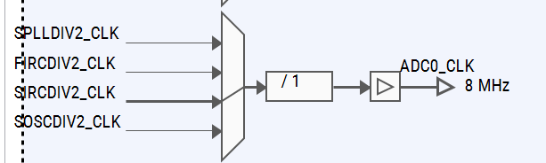
ADC Clock in S32K144 - Four available clock sources are mentioned below, but to learn about these clocks deeply you can refer clock peripheral blog.
- FIRC: Fast Internal RC (Resistor-Capacitor) Oscillator
- SIRC: Slow Internal RC (Resistor-Capacitor) Oscillator
- SPLL: System Phase-Locked Loop
- SOSC: System OSCillator
- Clock selection is managed by setting the CFG1[ADICLK] register.
- Regardless of the selected clock, its frequency must stay within the specified range for ADCK(2MHz-50MHz). If the available clock speed is too low, the ADC may not meet performance specifications. Conversely, if the clock is too fast, it must be divided to fall within the required frequency range, adjustable via CFG1[ADIV] to a division factor of 1, 2, 4, or 8. For specific ADC frequency requirements, refer to the device Data Sheet.

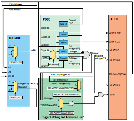
-> In ADC systems, triggers are signals that start the conversion process for the complete ADC block(ADC0 or ADC1), while by pre-triggers we mean the ADC channels of the ADC instance, whose conversion has to be done before the conversion of the whole ADC instance begins. Now there are 2 types of ADC Triggers in S32K1xx MCU:
- ADC Software Trigger: By writing some bit value to ADC peripheral Register, after that ADC conversion is started.
- ADC Hardware Trigger: By configuring some external ADC hardware event and after that ADC conversion starts
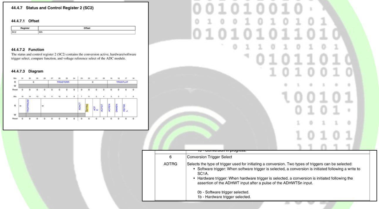
ADC Software Triggering:
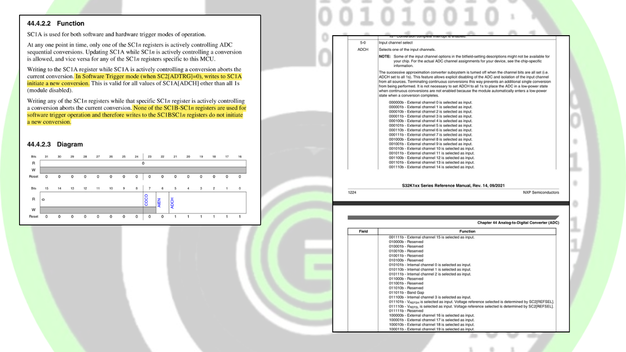
- By writing bit value to ADC Peripheral registers. SC1A and its last 6 bits. In last 6 bits we put value of which ADC channel we want to start the ADC conversion.
ADC Software Trigger ADC Hardware Triggering
-> ADC triggers and pre-triggers conversions we can start via hardware external events through use of, the Programmable Delay Block (PDB) or Trigger Multiplexer (TRGMUX).
PDB Triggering: PDB peripheral is provided specifically for trigger support in ADC. It triggers ADC conversions and controls channels via up to 8 pre-triggers( meaning 8 ADC channel pins), reducing CPU involvement. Each PDB pairs with an ADC (PDB0-ADC0, PDB1-ADC1).
TRGMUX Triggering: As we understood how PDB is an ADC-specific peripheral for triggering, similarly TRGMUX is a triggering peripheral for all peripherals available in MCU. TRGMUX also offers flexible ADC triggers using external/internal signals. Modules like CMP, LPIT, RTC, and LPTMR can trigger the ADC. TRGMUX enables different peripherals to start ADC conversions without the PDB.
-> The trigger source is controlled by SIM_ADCOPT[ADCxTRGSEL], allowing the selection of PDB or TRGMUX based on application needs.
- So its PDB is specially for ADC triggering and TRGMUX is for triggering of all peripheral.
- So we will use PDB to trigger ADC and PDB will be triggered through TRGMUX and TRGMUX will be connected to other peripheral for hardware inputs.
-> Hardware Triggering Schemes:
Default Scheme (PDB): The most common method is using the PDB to trigger the ADC. This approach is suggested for general use because of its simplicity and automatic trigger mechanism made dedicatedly for ADC.
Alternative Scheme (TRGMUX): TRGMUX provides another option for hardware triggering, offering more flexibility in selecting which peripherals or pins will initiate ADC conversions.
-> The SIM_ADCOPT[ADCxTRGSEL] field is used to control and configure the source of ADC triggers, allowing the system to choose between PDB or TRGMUX based on the application’s needs.

> Selectable Voltage Reference: External or Alternate
- The ADC can be set to use one of two voltage reference pairs for conversions:
- VREFSH and VREFSL – These provide the reference voltage.
- Each pair includes:
- A positive reference (VREFSH) should be between the minimum reference voltage high and VDDA.
- A ground reference (VREFSL) at the same potential as VSSA.
- Each pair includes:
- VREFSH and VREFSL – These provide the reference voltage.
- The ADC can be set to use one of two voltage reference pairs for conversions:
- Reference options:
- External reference pair: VREFH and VREFL.
- Alternate reference: VALTH, which can be an additional external pin or an internal source, based on the MCU configuration.
- Reference options:
- The reference source is selected using
SC2[REFSEL]. Refer to the specific MCU’s configuration details for more on voltage reference options.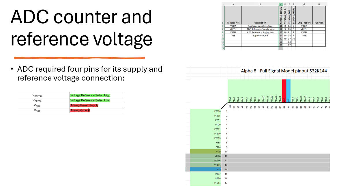
ADC Reference Voltage selections


- Function of the Register
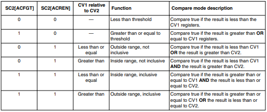
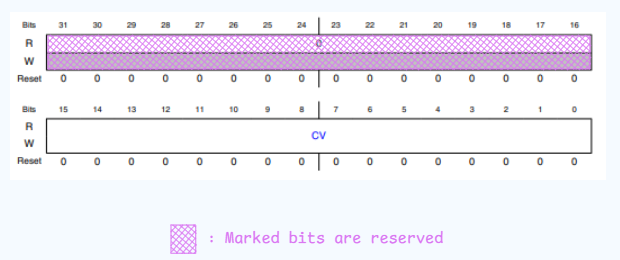
The Compare Value Registers (CV1 and CV2) hold values used to compare against ADC conversion results when comparison is enabled (SC2[ACFE] = 1).
- Same Format as Rn: CV1 and CV2 have the same format as the data result (Rn) registers.
- Using CV2: CV2 is only used if the compare range function is enabled (SC2[ACREN] = 1).
- Field of the Register
- CV: Compare Value
- Function of the Register