What is a Processor
Processor is programmable electronic circuitry that performs operations according to the instructions stored in memory. The processor as of itself does not have the memory and I/O devices. The processor reads the instructions stored in the memory, interprets it, and stores the output in memory or signals the I/Os. Processor Consists of the Processor core which contains circuitry for instruction fetching, decoding, and execution, register banks, and control units.
According to the architecture design of the processor, the different processors have different components. For example, ARM cortex-M4 processors have NVIC, MPU, Floating point units, optional debug subsystems.
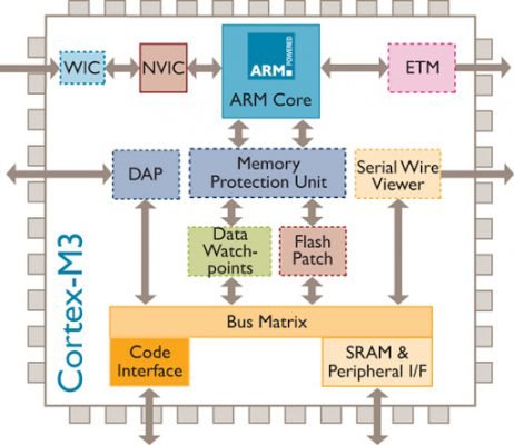
Fig 1.1 – Block Diagram of the Cortex-M3 and Cortex-M4 Processor.
The processor is the part of the Microcontroller and not a microcontroller as a whole and it takes only a small part of the silicon area. Processor design companies design the processors and various components that silicon designers need and license these designs to various silicon design companies including microcontroller vendors. These designs are called Intellectual Property (IP) and the business model is called IP licensing. Although many microcontroller vendors use ARM processors as their choice of CPU, the memory system, memory map, memory size, and peripherals can be completely different from one product to another.
This allows the microcontroller vendors to design differently. A block diagram of the microcontroller.
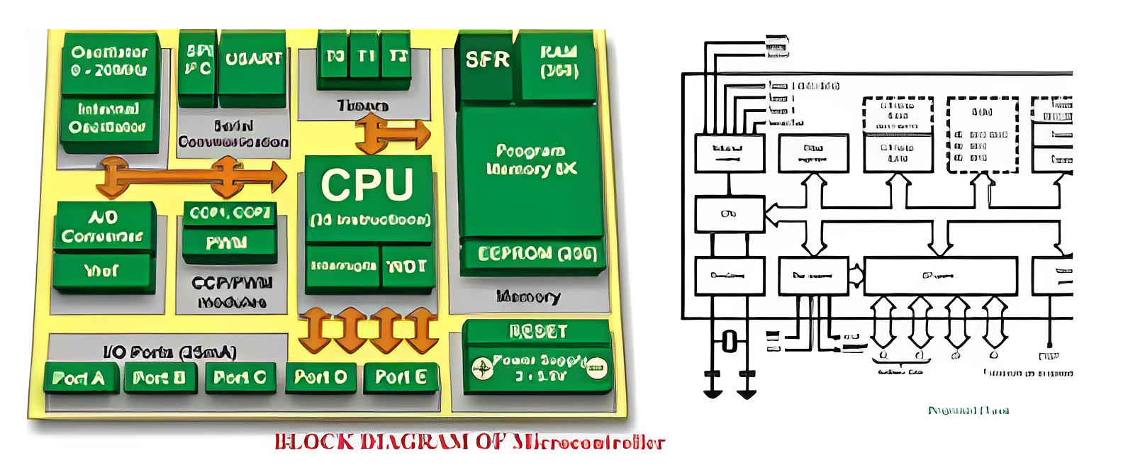
Fig 1.2 – A microcontroller contains Many different blocks
How does Processor control the world?
Processors become an integral part of our life. We come across many devices which have processors embedded in them. For example:
- The smartphone on which I am writing this article has ARM cortex-A55 and cortex-A75 as processor,
- The Famous Tesla motors FSD Self-driving computer has many ARM processors.
To give the idea of how processors are running the world look at these two examples.
- Upto 2019, Arm partners have shipped more than 160 billion Arm-based chips.
- Due to the shortage of semiconductor chips(processors) many car manufacturing companies had to reduce the number of cars manufactured.
ARM Processor
ARM processors are designed by ARM Ltd., ARM does not manufacture processors or sell the chips directly. Instead ARM licenses these designs to other semiconductor companies so that they can make their processor, microcontroller, SOCs as ARM processors are configurable. In the Cortex processor range, the processors are divided into three profiles:
1) The A Profile is designed to handle complex applications such as high-end embedded OSs.
2) The R profile processors are targeted primarily at the high end of the real-time market. These are applications, such as hard drive controllers, automotive systems, etc.
3) The M profile processors target smaller-scale applications such as microcontrollers and mixed-signal design.
ARM develops new processors, new instructions, and architectural features are added from time to time, as a result, there are different versions of the architecture. For example:
- ARM7TDMI is based on the architecture version ARMv4T.
- ARMv5TE architecture was introduced with the ARM9E processor families.
- With the ARM11 Processor family, the architecture was extended to ARMv6 with memory system features and SIMD instructions included.
- Cortex family processors are based on ARMv7 and ARMv6.
The cortex-M3 and cortex-M4 processors are based on ARMv7-M architecture. The architecture evolution of the ARM can be seen in the following (Fig 1.4). All the cortex-M processors support Thumb-2 technology(16-bit and 32-bit instructions), with no need to switch the processor between Thumb state and ARM state.
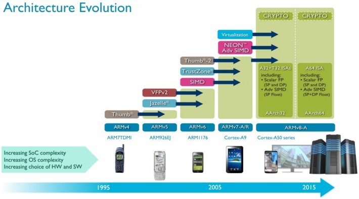
Figure 1.4 : Evolution of ARM
Figure 1.5
STM32 series is shown
How to ARM Processor based MCU's ?
The language used to program MCU is C/C++, but mostly C is used. There are many development suites available from open-source free tools, to budget low-cost tools, to high-end commercial, to mcu vendors propiatery IDE’s. packages. Some development toolchains are:
For Programming and debugging ARM Processor based MCU’s, we will be using Microcontrollers of different vendors like: STMicroelectronics and NXP Semiconductors.
We will be using STM32 Family of STMicroelectronics and S32 Family of NXP Semiconductors. Both of these are based on ARM Processor and have rich set of features and specifications which are ideal for learning embedded systems.
Now both the companies provide their own IDE’s for : STM32CubeIDE and S32 Design IDE for respective family of MCU mentioned above.
Or we can also use the Above-mentioned IDE’s which are general IDE’s can be used to program any ARM processor based MCU. But recomended one is to use Vendor specific IDE as it has many extra featutes for programming.
CMSIS
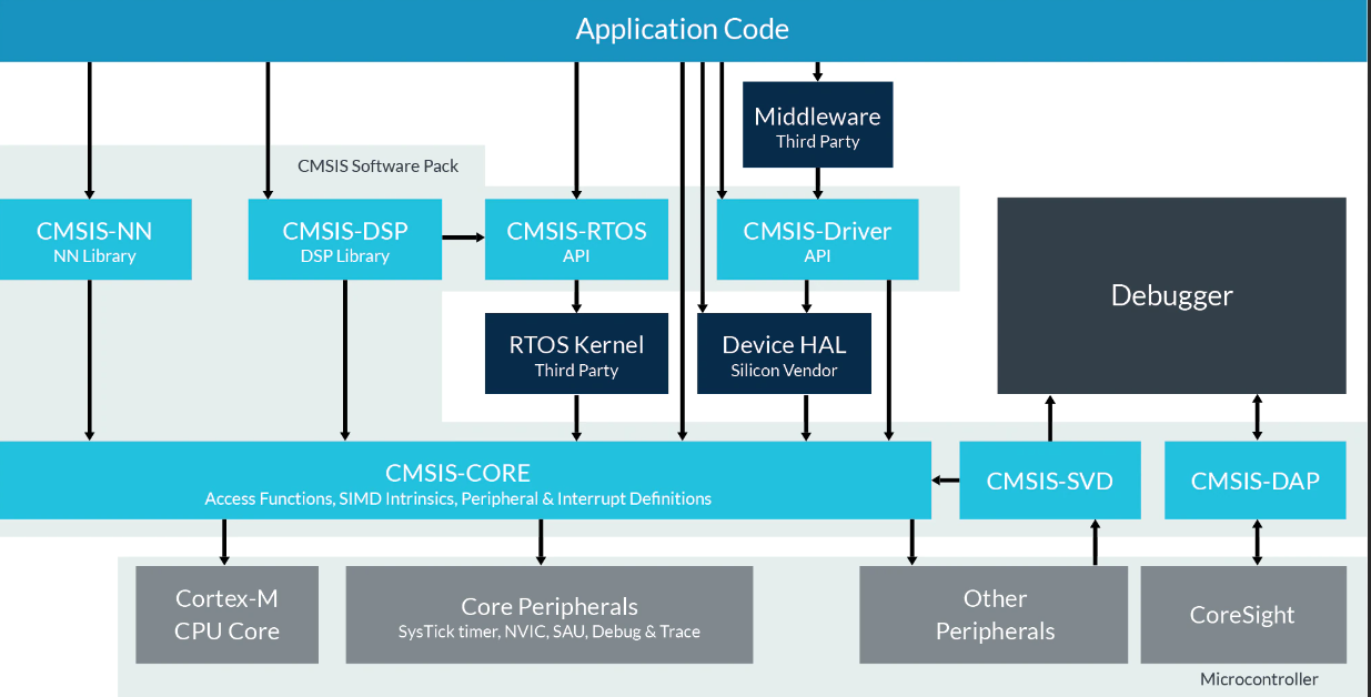
The Common Microcontroller Software Interface Standard(CMSIS) was developed by ARM to allow microcontroller and software vendors to use a consistent software infrastructure to develop software solutions for cortex microcontrollers.
THE AIM OF CMSIS:
- Software reusability: make it easier to reuse code with different Cortex-M processors, reducing time to market and verification efforts.
- Software compatibility: Due to consistent software infrastructure, software from various sources can work together, reducing the risk in integration.
- The CMSIS allows easy access to processor core features from the c language.
- CMSIS-compliant device drivers can be used with various compilation tools.
CMSIS started out as a way to establish consistency in device-driver for the Cortex-M microcontrollers, and this has become CMSIS-Core.
Since then, additional CMSIS projects have started:
A set of APIs for applications developers to access the features on the Cortex-M processor regardless of microcontroller devices and toolchain used.
This library is intended to allow software developers to create DSP applications on Cortex-M microcontrollers easily.
the System View Description in an XMl-based file format to describe peripheral set in microcontroller products.
the CMSIS-RTOS is an API specification for embedded OS running on Cortex-M Microcontrollers.
the CMSIS-DAP(Debug Access Port) is a reference design for a debug interface adaptor, which supports USB to JTAG/Serial protocol conversions.
The CMSIS files are integrated into device-driver library packages from the microcontroller vendor. So when you are using CMSIS-compliant device-driver libraries provided by the microcontroller vendors, you are already using CMSIS.
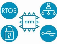
We can define the CMSIS into multiple layers:
Name definitions,address definitions, and helper functions to access core registers and core peripherals. This is processor specific and is provided by ARM.
Name definitions, address definitions of peripheral registers etc. This is device specific.
Access Functions For Peripherals
How do I use CMSIS-Core ?
Add Source files to the project. This includes:
- Device specific, toolchain-specific startup code, in the form of assembly or C.
- Device-specific device initialization code(e.g. System_c).
Add header files into the search path of the project:
- A device-specific header file for peripheral registers definitions and interrupt assignment definitions(e.g., .h)
- A device-specific header file for functions in device initialization code(e.g, system_.)
- A number of processor-specific header files(e.g, corre_cm3.h,core_cm4.h)
- Optionally additional vendor-specific header files for peripheral access functions.
The IDE automatically sets up the startup code for you when you create a new project. Otherwise, you just need to add the startup code from the device-driver library to the project manually. Startup code is required for the starting sequence of the processor, and it also includes the exception vector table definition that is required for interrupt handling.
STM32 HAL is an abstract lawyer ensuring minimized portability across the STM32 Portfolio. HAL APIs are available for all peripherals. These hide the MCU and peripheral complexity from the end-user.
Low-Layer APIs(LL) offer a fast lightweight layer that is closer to the hardware than the HAL. LL APIs are available only for a set of peripherals. These require deep knowledge of the MCU and peripheral specifications.
CONCLUSION PARAGRAPH: In this article, we just scratched the surface of the embedded world. In the upcoming articles, we will learn embedded development by doing projects.
Next Blog To Read for STM32
GPIO Peripheral in STM32F103 MCU
Table of Contents GPIO Theory So now we’ll talk about GPIO pins . GPIO stands for general purpose input output pins; they are the means for communication between the microcontroller and the external world (using sensors etc).It is signal that arrives on these pins or a signal that is sent or written on these pins that facilitates this communication. These pins can be configured to act as input or output via the application software(in our case stm32cube ide). The programmer can configure the pins as LOW or 0V or HIGH or 3.3V(or 5V ). These GPIO pins can also be configured to act as special purpose pins as well where their alternate functionality is exploited . These alternate functionality includes UART , ADC , SPI etc . In the case of UART communication, Transmitter(Tx) and Receiver(Rx) pins are required. GPIO pins can be configured to act as TX or RX pins . Even in ADC the pins are configured to act as Analog pins having 12 bits of resolution . The alternate functions of various pins are shown below: Input floating Input pull-up Input pull-down Analog Output open-drain Output push-pull Alternate function push-pull Alternate function open-drain GPIO Peripheral in STM32F103 All the pins of STM32F103 are grouped in multiple ports as PORT A, PORT B, PORT C As can be seen from Pin configuration chart in the PA1 stands for Port A Pin 1. There are 37 GPIO pins in stm32f103 which are divided as PORT A with 16 pins, PORT B with 16 pins, PORT C with 3 pins and PORT D with 2 pins. Each GPIO port has two 32-bit configuration registers (GPIOx_CRL, GPIOx_CRH), two 32-bit data registers (GPIOx_IDR, GPIOx_ODR), a 32-bit set/reset register (GPIOx_BSRR), a 16-bit reset register (GPIOx_BRR) and a 32-bit locking register (GPIOx_LCKR). In the register names, x stands for the port to which pin belongs. If we are configuring pin PA1, it has Port A then registers would be accessed by GPIOA_CRL and etc. Out of above-mentioned registers, GPIO peripheral has 2 most important registers: Direction Register(GPIOx_CRL, GPIOx_CRH)</h3 > Direction register: Set the corresponding pin as input/output pin. Data register(GPIOx_IDR, GPIOx_ODR)</h3 > Data register: where we set the Logic level (High (1)/Low (0)), for the corresponding pin if it is configured as output pin or we read the Logic level (High (1)/Low (0)), for the corresponding pin if it is configured as input pin. Pin Configuration Chart Pin Definitions GPIO Peripheral Block Diagram in STM32F103 First after selecting the pin the port is decided Then after following the arrow the busses are selected based on it: APB/APB1 or AHB After which the clock is enabled to the particular port using either __HAL_RCC_GPIOX_CLK_ENABLE() function or using the RCC AHB1 peripheral clock enable register and selecting the port to which clock has to be provided by enabling it. Methods to configure the GPIO Peripheral Configuring the busses i.e AHB1, AHB2, APB1, APB2 . The AHB bus is faster than APB bus and in case of certain modules they are connected to the same bus .Hence it depends upon the application which bus to use. As can be seen from the picture below the AHB1 takes clock to PORT A , PORT B , PORT C etc . Hence to initialize a pin to a particular port the in RCC AHB1 clock enable register GPIOEN is set to 1 (For Port A GPIOAEN , For Port B GPIOBEN etc) Enabling the clock to that port otherwise the particular pin will not be functional Creating an instance of the structure and then using the members of the structure set the following:- PIN – Takes the pin no as input GPIO_PIN_X {where X -0 to 15} MODE– Selects the mode the specified pin is supposed to work in . It takes in value Output Push Pull ,Output Open drain PULL- It selects the initial value of the pin and takes value no pull up no pull down, pull up or pull down SPEED- Selects the speed of the working of the specified pin i.e low, medium or high ALTERNATE- Specifies the alternate function performed by the pin UART TX OR RX , ADC etc, GPIO Peripheral SDK using STM32HAL We are going to use STM32 HAL SDK for using the GPIO peripheral of the STM32F103. STM32HAL is a very versatile and robust Software package for using Peripherals of the STM32 Microcontroller family. To know more about STM32HAL, refer to this link. Each STM32 HAL has drivers for all the peripherals of the STM32 Microcontroller(One can navigate to the Driver folder in the STM32F1 HAL local repo installed). These drivers can be configured and enabled to use in the project via the STM32 CubeMX configuration tool, which is also integrated into STM32CubeIDE( just like told in the above section for configuring GPIO peripherals). Will be digging into that part, in the next section. For now, let’s understand the STM32HAL GPIO SDK for STM32F103 MCU. stm32f1xx_hal_gpio.c: This file consists of various macros and is responsible for the intialization and configuration of the functions which in turn configures the peripheral. stm32f1xx_hal_gpio.h: consists of various structure definitions that help configure various parameters of the pin, enumeration, and various macros stm32f1xx_ll_gpio.c & stm32f1xx_ll_gpio.h: GPIO Low-level driver source/header file, contains functions that configure the GPIO Peripheral registers at the hardware level. These files are the ones that actually interact with the hardware and make it configurable to our needs.  STM32 HAL Functions for GPIO Peripheral Functions are set of instructions that required to perform certain tasks. In general, a function is first declared in header file(.h) and then it is definied in source file(.c) and then called in main.c or application code. It is of the form function return data type, function name and function arguments. In Embedded functions are required to initialize a peripheral or configure it on the basis of various parameters which are passed on using arguments. This information is then passed on to the registers. List of functions used
STM32F103 & ADC: Single Channel Conversion
In the last post, we have gotten to know about the features of ADC Peripheral that we have in STM32 MCU. Now in this blog with the series of bare Metal Programming for Blue Pill, we will understand different register bytes and bits of ADC Peripheral to be used for using it in different features, configurations, and modes as we get to know about in the Previous Post. In this blog, we will be going through how to use ADC Peripheral for converting a Single Channel of ADC (only one ADC pin) and see its bare metal code. Single Channel Conversion Mode: Only one ADC pin is used, this mode is like when we have say connected only one analog sensor to one of the ADC pins of MCU like the Potentiometer is connected at PA0 pin. ADC Registers In depth for: Let\’s get into an in-depth understanding of which registers and their bits are used for configuring the ADC peripheral of Blue Pill in Single Channel Configuration. We will focus on bits and will give an explanation of why those bits are used for the 1. ADC_SR(ADC status Register) –>This register tells the status of ADC channel Conversion, as it name says. STM32F103 ADC Status Register: 11.12.1 Bit 1[EOC ]: This bit is set by hardware when a single channel of any group (Regular or Injected) is converted successfully. So this bit is used for monitoring when the ADC conversion is completed by using it inside the while loop if interrupts are disabled. 0: ADC Channel Conversion is not completed 1: ADC Channel Conversion is completed When hardware set this bit, we can clear this bit from the firmware end by setting the bit to 0 or by reading ADC_DR(ADC Data Register) Bit 4[STRT]: This bit is set by hardware when regular channel conversion has begun. So when we start the Regular Channel Conversion, we will use this bit inside the while loop to check that whether Regular Channel conversion has started or not. 0: No regular Channel Conversion has started 1: Regular Channel Conversion has started When hardware sets this bit, we can clear this bit from the firmware end by setting the bit to 0. Even if we don\’t clear this bit it will cause no effect during ADC Conversion. But its good practise to clear all bits of Status Register before starting the new conversion 2. ADC_DR(ADC Data Register) –> This register stores the converted digital data at a 12-bit resolution of the converted ADC channel. STM32F103 ADC Data Register 11.12.14 Bit 15:0 [DATA 15:0]: The ADC_DR is divided into two 16 bits groups. The first 16 bits from 0-15 contain the Converted value of the configured ADC Regular Channel. As our ADC is of 12-bit resolution, so this is left aligned or right aligned to 4 bits so as to get the 12 ADC converted data . Left Aligned or Right alignment of ADC Data Depends on ALIGN bit of ADC_CR2 So we will have following code and algorithm for ADC_SR & ADC_DR register:while(!(ADC1->SR & ADC_SR_STRT)) while(!(ADC1->SR & ADC_SR_EOC)); // wait till a group channel converstion has completed adc_data = ADC1->DR; //clear the EOC bit by reading DR register ADC1->SR &= ~ADC_SR_STRT; 3. ADC_CR1(ADC Configuration register 1) –> This register is used for the Configuration of ADC peripheral for Analog Watchdog Discontinuous Mode Interrupt Enable/disable Dual Mode configuration Scan Mode As we are not using any of these features, so all the bits for these registers will be set to zero, and to know about these features and their bit functions, u can navigate to corresponding blogs for those. STM32F103 ADC Configuration Register 1. 11.12.2 Bits 19:16 [DUALMODE 3:0]: These bits are used to configure the type of operating mode. In the blue pill, we have two ADC peripherals: ADC1 & ADC2. We can use these 2 ADC peripherals simultaneously by configuring the respective ADC in different modes or in independent modes. We are going to use these ADC in independent mode as will be using only ADC1 peripheral, so DUALMODE[3:0] will be set to 0. Bit 8[SCAN]: This bit is used to enable/disable the SCAN Mode feature in the ADC peripheral of BLUEPILL. Scan Mode is used when we convert more than 1 channel to scan all the configured channels in a Regular Group. As we are using only a single channel, means only one ADC pin is used so SCAN mode is not used and this bit will be set to 0. 0: Scan Mode disabled. 1:Scan Mode Enabled. So we will have following code and algorith for ADC_CR1 register:ADC1->CR1 &= ~(ADC_CR1_SCAN); // SCAN DISABLED, if using scan mode then dma must be enabled ADC1->CR1 &= ~(ADC_CR1_JDISCEN | ADC_CR1_DISCEN); // Discontinous mode disabled for both injected and regular groups ADC1->CR1 &= ~(ADC_CR1_DISCNUM_2 | ADC_CR1_DISCNUM_1 | ADC_CR1_DISCNUM_2 ); // no channels are configured in discontinous way. // if discontinous mode is enabled then number of //conversions to be done by discontinous mode has to be configured // DISNUM bits ADC1->CR1 &= ~(ADC_CR1_DUALMOD_0 | ADC_CR1_DUALMOD_1 | ADC_CR1_DUALMOD_2); // INDEPENDENT MODE SELECTED ADC1->CR1 &= ~(ADC_CR1_AWDEN | ADC_CR1_JAWDEN); // Analog watchdog disabled for both groups: regular and ibnjected 4. ADC_CR2(ADC Configuration Register 2) –> This register is used for the configuration of ADC Peripheral for: ADC Conversion enables/disabled for regular and injected groups and ADC peripheral enable/disable. Trigger source configuration for regular and injected groups. ADC Data Alignment, DMA, Continous, temperature sensor setting. STM32F103 ADC Configuration Register 2 11.12.3 Bit 0 [ADON]: ADC Peripheral On/OFF. This bit will be set to 1 to enable the ADC peripheral. All channel configurations and ADC Peripheral configurations have to be made before setting this bit to 1. 0: Disable ADC Peripheral 1: Enable ADC Peripheral Bit 1 [CONT]: This bit configures between Single Conversion mode and Continous Conversion mode. Continuous Conversion mode is selected when we have more than 1 ADC channel to be converted. As in this blog, we have
PWM on STM32F103
What is PWM? PWM or Pulse Width Modulation, is a type of digital electrical signal which is periodic in nature, with a rectangular waveform. There are certain terms associated with PWM which we need to understand before we move ahead. Here’s a graphical representation of a PWM signal- · ‘Period’ = Tp , is the time it takes to repeat the same waveform · ‘Duty cycle’ is the time for which the signal is a logic 1 by the total time period. Ton is the time for which the pulse is high Hence, Duty cycle % = (Ton/ Tp) X 100 · ‘Frequency’ = F is the number of times the waveform repeats in a second. So, F = 1/Tp. Applications of PWM signals PWM signals have an extremely wide range of applications, here are a few of them- · Variable voltage generator– if you vary the duty cycle of a PWM signal and apply it to certain electrical components, the components act as if they are receiving analog signals. This is because the response time of the components is finite. So, components like LEDs, buzzers, brushed DC motors etc. can be controlled by PWM signals. Meaning, you could control speed of a motor, brightness of an LED or amplitude of a buzzer and so on. The voltage that they receive has a linear relationship with the duty cycle. So, if logic 1 is 5 Volts 0% duty cycle – 0V 25% duty cycle – 1.25 V 50% duty cycle – 2.5 V 75% duty cycle – 3.75V 100% duty cycle – 5V · As a control signal – Some electrical devices/components analyze PWM signals that they are receiving to give a corresponding output. So, changes in the duty cycle are reflected in the output. These include Servo motors, electronic speed controllers (ESCs) and many more. Here, the devices respond only to specific PWM duty cycles and frequencies If you take the example of servo motors, they can only be operated at 50Hz signal with a duty cycle of 2.5 % to 12% . Anything beyond that doesn’t result in the movement of the servo. (The frequency and duty cycles vary from among different servos, this is a very common value which most 180-degree servos respond to) Similarly, ESCs respond to a PWM signal with ON time of 1ms for minimum throttle and 2ms for maximum throttle with PWM frequency of 50 Hz. Some devices such as HCSR04 ultrasonic sensors give an output as a PWM signal in which the pulse width corresponds to the time it took for the ultrasonic wave to be received. How is PWM signal Generated on STM32?? Timer peripheral STM32 blue pill has 15 pins which can generate a PWM signal, with other models having even more pins for PWM generation. In this section, we will try to understand how PWM signals are generated by STM32 Every microcontroller has a built-in circuit which can measure the passing of time. These are called Timers. What timers essentially do is count up to a certain number and upon reaching that number, they change the value of a certain register to indicate that the timer has counted up to that number. Now, the time it takes to increment this count by 1 is determined by the timer’s clock frequency. So, if the frequency of a timer is 1KHz, its time period will be 1 Millisecond. Hence, if we count up to 10, we have measured the passing of 10 Milliseconds. This is how, by simply incrementing a number, timers can measure the time that has passed since the timer began counting. (This is how the HAL_Delay() function generates delays) The maximum count a timer can make is determined by its register size. So, an 8 bit timer can count up to 28 = 256, 10-bit timer –210 = 1024 16-bit timer –216 = 65536 32-bit timer –232 = 4294967296 So, a 1 bit increase in timer size equals to double the count Timers are extremely necessary for the functioning of a microcontroller as a lot of events in programs are time based, which you may not even realize. Timer Peripheral modes and features Coming to STM32 Blue pill, it has 4 timers of 16-bit size. To perform these functions, they need to be in specific modes. Here are all the modes in which timers can operate in STM32- 1. Input capture mode– In this mode, a pin on the board is set as input on which a PWM signal is sent by some device and we measure the frequency and duty cycle of that signal. This can be used to interface with devices such as HCSR04 ultrasonic sensors, which send a PWM signal as input to the microcontroller, where different parameters of PWM signals can be used to determine the distance which the sensor is trying to measure. 2. Output compare mode– In this mode, the timer is used as a counter and the count is compared to a register which contains a pre-programmed value, when they are equal, a software interrupt is generated and using this, a given pin is switched high or low. This mode comes in very handy when you are making a project which requires you to use multiple peripherals and at the same time generate a rectangular waveform of a given frequency and duty cycle, as it is interrupt based. 3. One pulse mode– In this mode, a pulse can be generated based upon a trigger from an input pin on the board , the pulse generation takes place after a certain delay from when the input trigger pulse was detected. This can be considered as a combination of mode 1&2 (IC &OC) 4. PWM generation mode– In this mode, we can generate a PWM signal on a given pin by fixing a frequency and a duty cycle. This is the mode we will be using to generate PWM signals through the main loop. The difference of this mode to mode 2 (Output compare
Blogs to read for ARM Processor
Automotive Microcontroller programming training session at DTU College
We have successfully conducted a 10-day training program on Automotive Microcontroller Programing at Delhi Technical University from 6th December to 15th December. The training program was attended by Btech Students of ECE branch and some students of Mtech branch. List of attendance as per dates are: 06/12/2024:25 07/12/2024:25 08/12/2024:23 09/12/2024:22 10/12/2024: Holiday by students 11/12/2024:23 12/12/2024: 22 13/12/2024:19 14/12/2024:15 15/12/2024:10 The 10 day training program session start by introducing students with the Microcontroller Technology. On day 1 of the training session students were made to taught microcontroller technology. General overview of what is semiconductor industry, how does semiconductor industry works and different kind of companies in semiconductor industry. Followed by in depth exploration of microcontroller technology, which is one of the kind of semiconductor chip. Diving into Building block, Functional block, Hardware Development Kit and Software Development Kit of Microcontroller Technology. In the end we conclude the day by discussing about Industrial Microcontroller like that of NXP, Renesas, Infenion giving students exposure to MCU’s apart from Arduino/ESP frameworks. We very much focus on NXP S32K144 MCU which is an automotive MCU and get handson feel with Its Development Board ElecronicsV3 and SDK of S32 Design Studio On Second day we followed by exploring and diving deep into automotive technologies. How Automotive Industry works, Different companies involved in it and overview of Automotive technologies like Functional Domain, E/E Architecture and Autosar Software Tech Stack. On this we very much deep dive into Autosar Software Tech stack and give stduents overview on how to start with it. We start by exploring the MCAL Layer technology of Autosar Software Tech Stack and set up its Software environment using S32 Design Studio IDE and its software package installation. On Day 3-4 we started with Handson experiment after getting initial overview of technologies. On Day 3 & 4 students explored the GPIO/PORT peripheral in Microcontroller technology, students were given in depth overview and understanding on how this peripheral works, why is it used, how to use it and its applications. Students were made to taught about this peripheral from Microcontroller datasheet and made to understand different specs/features of this peripheral from MCU documents. After that students were made to taught how to use this peripheral in Automotive Microcontroller by making them understand on its peripheral stack using Autosar MCAL Driver specs. Students were made to taught how to use Autosar Code configurator tool for GPIO/PORT peripheral. They were taught how to use Software API’s, what parameters to send on those API’s an in which chronology those API’s need to be used. In the end students were given time to learn and have Handson with Embedded Softwrae Debugging of microcontroller. They were made to develop different functional demo codes on GPIO/PORT peripheral and taught how to do embedded software debugging for it. Day 5 was holiday: After continous 4 days of technical learning and information, students asked for day off. Number of students on that day have interviews and assessments so day off on this day was taken. Day 6-7: we started with Handson experiment of ADC peripheral of microcontroller technology. We started by getting overview on what is ADC peripheral, how does it work, why is it needed and different specs/features of ADC peripheral in MCU’s. After that we deep dive into NXP S32K144 concentric ADC peripheral. We explored how ADC peripheral works in S32K144 MCU using its datasheet and exploring its peripheral register’s. After that students were made to taught how to use ADC peripheral in Automotive Microcontroller by making them understand on ADC peripheral Driver using Autosar MCAL Driver specs. Students were made to taught how to use Autosar Code configurator tool for ADC peripheral. Understanding and exploring its different menu sections, sub menu sections. Which sections to configure, how to configure and why to configure. They were taught how to use Software API’s of ADC Driver stack, what parameters to send on those API’s an in which chronology those API’s need to be used. In the end students were given time to learn and have Handson with Embedded Softwrae Debugging of microcontroller for ADC Peripheral. They were made to develop simple functional demo codes of reading POT values using ADC peripheral and taught how to do embedded software debugging for it. Day 8-9: On these 2 days students were made to taught PWM Peripheral of Microcontroller technology. How PWM signals are generated, how they work , different sepcs/features of PWM Signals. Students were made to introduce the concept of TIMER peripheral in MCU’s which is used to generate PWM signals via it. In these 2 days students were also made to get familarize with Logic Analzer tool which is used to capture PWM Signals. Students were made to understand TIMER peripheral of NXP S32K144 Automotive MCU, how it works and how to use it for generating PWM signals. Followed by theory and hardware overview of PWM signals, students were made to do Handson exploration by generating PWM signals of different frequency/duty cycle using PWM Driver stack of Autosar MCAL Layer. After that students were made to taught how to use TIMER peripheral in Automotive Microcontroller by making them understand on PWM peripheral Driver using Autosar MCAL Driver specs. Students were made to taught how to use Autosar Code configurator tool for PWM Driver. Understanding and exploring its different menu sections, sub menu sections. Which sections to configure, how to configure and why to configure. They were taught how to use Software API’s of PWM Driver stack, what parameters to send on those API’s an in which chronology those API’s need to be used. In the end students were given tasks to generate PWM signals of different frequencies and duty cycle. On the last day, students were instructed to do Integration of What all thinsg they have learned so far. They were given task to Combine all Peripheral of Automotive MCU which was taught as if now in a single project. They did a task of using GPIO, PORT, ADC & PWM Peripherals
SPI Peripheral in S32K144
Explore this blog to know about SPI peripheral in NXP S32K144 MCU
UART Peripheral in Microcontroller
Explore this blog to know about UART peripheral in Microcontroller for doing UART communication
SPI Communication in Microcontrollers
Explore this blog to know about SPI peripheral in Microcontroller for doing SPI communication
TIMER Peripheral in Microcontroller’s
Explore basics of TIMER Peripheral in Microcontroller!!
ADC Peripheral in Microcontroller’s
Explore about ADC peripheral in Microcontroller from foundational and functional level
Author: Kunal Gupta
Author