
Table of Contents
 W25Q128JV SPI Flash Memory interfacing with STM32 and AVR MCU
So hello guys, welcome back to the Gettobyte once again. As I have told you that we are going to start with application codes also, so now in this blog what we are going to do?? We are going to interface the W25Q128JV SPI Serial flash memory module to our STM32 MCU and AVR8 MCU.
Now let\’s look at how this module looks. This module is very small and packed into small sizes. One can buy it easily from the Amazon Website. This module has 6 pins: VCC, GND, and 4 SPI Communication pins( MOSI, MISO, CE & SCK). But the IC has much more pins, that I will be briefing below.
 W25Q128JV SPI Flash Memory module
Now starting with this Flash memory, In this blog, I will be telling you about its:
- General description of the IC.
- Features of this Serial Flash Memory.
- Pin Description.
In the next subsequent blogs will be making the application code on AVR and STM32 MCU using SPI peripheral and peripheral driver. At first, will be making the application code on AVR MCU and then on STM32 MCU. So now moving forward, let\’s begin our journey to it.
General Description of W25Q SPI flash memory
So starting with W25Q128JV. These are the Serial communication-based Flash memories into which we can store data. These can work as RAM memory for memory constraint embedded MCUs. We can transfer data from these memory chips in standard SPI serial communication up to a frequency of 133 MHZ and when used in Dual/Quad SPI Serial communication, data transfer frequency can go up to 236MHZ/532 MHZ. So one can read, write and fetch data from these memory chips at very high frequencies.
These have 65536 programmable page lengths and in total there are 256 pages. That means it has 256 pages and on each page, we can write 65536 bytes.
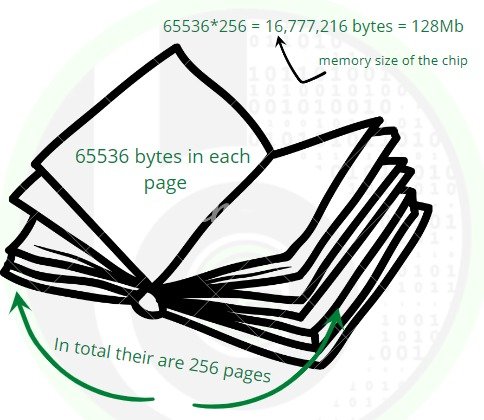 W25Q SPI flash memory depicted as a book
On each byte of these pages, we can read and write at a redundancy of 10000 times. Up to 256 bytes can be programmed at a time. We will go into more detail when we will understand its block diagram of memory mapping and management.
Features of W25Q SPI Flash Memory
It can run on Standard SPI, DUAL SPI, and QUAD SPI.
Standard SPI: is traditional SPI Protocol which has CLK,CS,MISO(DO),MOSI(DI) pins. In this, we have 1 pin(MOSI) for sending data from Master to Slave and another pin (MISO) for sending data from slave to master. It can run at Max speed of 133MHZ for standard SPI. To know more about SPI, refer to this blog
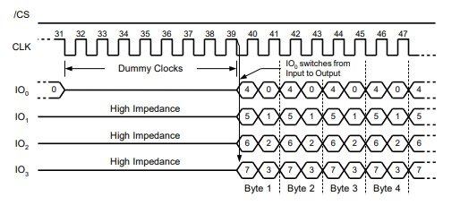
Dual SPI: In DUAL SPI, we have 2 Output/Input pins. Which means at a time we can send data from 2 pins and receive data from 2 pins. Refer the below image, DI becomes IO0 and D0 becomes IO1, so at a time we can send and receive data from both of those pins. As 1 byte has 8 bits and bits 0 and 1 of my one byte are being transmitted or received simultaneously, thus our data transfer becomes 2x then standard SPI, where only 1 bit is commuted at a time. In Dual SPI Max speed it can run at is 266 MHZ.
 DUAL SPI
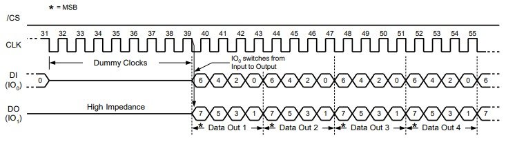
QUAD SPI: In QUAD SPI, we have 4 Output/Input pins. Which means at a time we can send data from 4 pins and receive data from 4 pins. IO0,IO1,IO2,IO3 are the 4 pins from which data is commuted between slave and master. In Quad SPI MAX speed it can run at is 532 MHZ.
 QUAD SPI
One can perform 100k program-erase cycles per sector and it has data retention for more than 20 years.
- Efficient continuously read for about 8/16/32 byte warp. Byte warp here means that it can read memory continuously in the chunks of 8/16/32 bytes in one single time. Lets say it is reading in 8 byte wrap, so at first read it will read 0-7 bytes, then in next 8-15 bytes, then 16-23 bytes.
- Then the other important thing is Advance Security features which this IC has. You will be able to understand these features in better way when we will go through the Status and Configuration registers of this IC. On the memory chip,
- We can lock the certain memory bytes, that is no one can write or read on configured memory bytes or size.
- We can use the OTP (one time password) to have password based memory protection
- We can access the memory bytes of the IC, in Blocks(64 KB), sectors(4KB) or single byte. Starting from the Top of memory or from the Bottom of memory.
PINOUT of the W25Q128 Flash memory chip
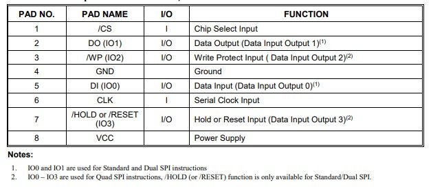
So W25Q128 has 8 pins. Depending on the package we have, the number of pins of the IC can increase or decrease. The module which we will be using is packaging WSON.
Pin number 1 is CE (Chip Select), used to select the SPI slave by making a LOW signal to this pin
Pin number 2 is DO (Data Output), that is MISO pin in case of standard SPI and IO1 in case of DUAL/QUAD SPI.
Pin number 3 is /WP (Write Protection pin) ( will tell you about it in the below section) and IO2 in case of Dual/Quad SPI.
Pin number 4 is GND (Ground).
Pin number 5 is DI(Data Input), that is MOSI pin in case of standard SPI and IO0 in case of DUAL/QUAD SPI.
Pin number 6 is CLK, the Clock pin of SPI communication.
Pin number 7 is /HOLD or /RESET pin ( will tell you about it in the below section) and IO3 in case of Dual/Quad SPI.
Pin number 8 is VCC.
Let’s just deep dive into the pin description of this IC
Chip Select is held high, that is master has not selected the slave and all my pins would be at High impedance. When the CS pin is held low, the master has selected the SPI slave and power consumption would be increased to intermediate levels. all of these serial data pins and CLK pins would be receiving or transmitting the data as per our configurations.
Serial Data Input, Output, and IOs (DI, DO and IO0, IO1, IO2, IO3): as I have told you that DI and DO are IO0 and IO1, these are the normal MOSI and MISO pins. If we have selected DUAL or QUAD SPI pins, then depending on that IO2 and IO3 would be used as serial communication pins or as /WP and /HOLD-RESET pins.
So in this module, we can use Standard SPI only because the pinout of IO2 and IO3 are not given in this module breakout. so we are going to use Standard SPI only.
Write Protect(/WP) is a pin that controls the writing on Status Register. WP pin set as HIGH –> Status register is unlocked and can be written. WP pin ser as LOW –> status register is locked and can not be written. If we are using QUAD SPI, then this pin would become my IO2 pin. Otherwise in Standard and DUAL SPI, it is used as a WP pin only.
Pin number 7 can be used as HOLD (/HOLD) or Reset(/RESET) pins, if not using QUAD SPI. In packages SOIC16 and TFBGA pin, 7 is used as the RESET pin. In this case, if the pin is driven low for a minimum period of ~1us, then the device will terminate any external and internal operations and returns to its power-on-state. In all other packages pin 7 is used as a HOLD(/HOLD) pin. In that case, the HOLD pin is used for pausing our ongoing operation by the hardware control. If we are using QUAD SPI, then pin 7 is used as the IO3 pin. By default, the W25Q128 module doesn\’t have pin 7 as a breakout pin. So will ignore this pin for our current scenario
So now the remaining things about the register description and block diagram will be there in the next blog.