Introduction
–> FTM(FlexTimer Module) is a peripheral that offers multiple functionalities: Input Capture mode(for recording input signal timing for frequency or duty cycle measurement), Output Compare(triggers events at specific timer counts for precise signaling), and PWM Generation(creates adjustable PWM signals for motor speed and power control). Our main focus will be on PWM Generation. The first question that comes to mind is “What is PWM?, and Why generate PWM?”.
–> What is PWM?
PWM or Pulse Width Modulation is a technique for controlling analog devices using digital signals. In PWM, the signal rapidly alternates between high (on) and low (off) states, creating a square wave. By adjusting the “on” duration, or duty cycle, we can effectively control the average power supplied to a device.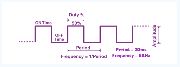
–> Why generate PWM?
PWM is essential in applications where precise control over power or speed is needed without complex hardware. For example, it’s widely used for controlling motor speed, LED brightness, and even power to heaters.
–> Important Terminology before Operating PWM
- Amplitude represents the peak voltage level of the signal.
- Duty Cycle is the percentage of time the signal remains high within one cycle, controlling how much average power is delivered to the device(If power output is 5 watts but with 50% duty cycle then power delivered will be 2.5 watts only).
- Frequency is the rate at which each cycle repeats, affecting how quickly a device responds, which is critical in motor control and other real-time applications. To calculate each cycle, just reciprocate and you get the Period of the signal.
–> After all this, only one thing is left which is”How is PWM generated”.
The first and most important thing to know is that the FTM peripheral is a counter-based timer peripheral that relies on the counters for PWM signal generation. there are 3 types of counters in the FTM peripheral that are responsible for setting period and frequency, let’s name them MAX Counter, THRESHOLD Counter, and VARIABLE Counter.
- MAX Counter (used to set the PWM period),
- Threshold Counter (defines the duty cycle), and
- VAR Counter (increments to trigger pin changes).
–> Cycyle of PWM Generation
Initialization and Counters Setup:
- MAX Counter: This counter is set to a specific value representing the full period of the PWM signal. For example, if MAX is set to 1000, the PWM period will complete after the counter reaches 1000.
- Threshold Counter: This is set to a value less than the MAX counter, controlling the duty cycle. For instance, setting the Threshold to 500 with a MAX of 1000 results in a 50% duty cycle.
- VAR Counter: This counter counts up from 0, incrementing with each clock pulse, to form the basis of the PWM timing.
PWM Signal Generation Cycle:
- Counter Starts: When the PWM is initiated, the VAR counter begins incrementing from 0. As it counts, the microcontroller pin initially remains low.
- Threshold Reached (Pin Toggled High): When the VAR counter matches the Threshold value, the FTM toggles the configured output pin high. This high state will persist until the VAR counter reaches the MAX value.
- MAX Counter Reached (Pin Toggled Low): When the VAR counter reaches the MAX counter value, the output pin is toggled low again, marking the end of the PWM cycle. The VAR counter then resets to 0, starting a new cycle with the same timing and pin changes.
Continuous PWM Waveform:
- With each cycle, this process repeats, creating a series of high and low states on the output pin. The duration of the high state relative to the period defines the duty cycle, which adjusts how much time within each period the signal remains high.
- By changing the Threshold value while keeping MAX constant, the duty cycle can be adjusted dynamically. For example, increasing the Threshold to 750 with a MAX of 1000 would create a 75% duty cycle, increasing the average output voltage.
Resulting PWM Signal and Control:
- This generated PWM waveform can be fed to devices like LEDs, motors, and MOSFETs to control their operation. The high time (duty cycle) determines the average power delivered: a higher duty cycle means more power and, for example, greater motor speed or LED brightness.
Now, we’ll move towards the feature of PWM.
Features of FTM
1. Concept of Counter in FTM
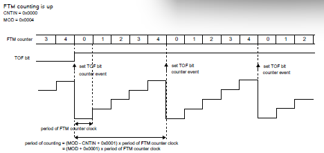
–> The FlexTimer (FTM) operates using a 16-bit counter that channels use for input or output functions. The FTM counter clock is derived from the selected clock, divided by the prescaler. It supports multiple counting modes:
Modes of Operation:
Up Counting:
- Selected when using Edge Align Mdoe(discused in further section)
- The starting value is defined by
CNTIN, and the final value byMOD. The counter starts atCNTIN, increments toMOD, then reloads withCNTINand repeats. - The period is calculated as:
Period = (MOD – CNTIN + 1) × (FTM counter clock period). - The
TOFbit is set when the counter rolls over fromMODtoCNTIN.
- Selected when using Edge Align Mdoe(discused in further section)
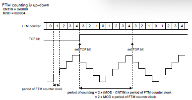
2. Up-Down Counting:
- Selected when using Center Align Mode(discussed in further section).
- The counter increments from
CNTINtoMOD, then decrements back toCNTIN, and repeats. - The period is:
Period = 2 × (MOD – CNTIN) × (FTM counter clock period). - The
TOFbit is set when the counter transitions fromMODtoMOD-1.
2. Channel Modes
| Field | Function | Typical Use Case |
|---|---|---|
| DECAPEN | Enables dual-edge capture mode. | Pulse width or period measurement. |
| MCOMBINE | Enables modified combine mode. | Generating more advanced PWM outputs (e.g., complementary PWM). |
| COMBINE | Combines two adjacent channels for PWM. | Producing complementary PWM for motor control (e.g., H-bridge). |
| CPWMS | Selects between edge-aligned or center-aligned PWM. | Reducing harmonics in motor control with center-aligned PWM. |
MSA : MSB | Select channel mode (e.g., PWM, output compare). | Configuring the channel for PWM or Output Compare mode. |
ELSA : ELSB | Defines output action (set, clear, toggle) on match. | Controlling whether a signal is set, cleared, or toggled on match. |

If I have to summarize the total mode of FTM:
Input Capture
Output Compare
Edge-Aligned PWM
Center-Aligned PWM
Combine Mode
Modified Combine PWM
Dual Edge Capture
1. Input Capture Mode of FTM
–> The Input Capture mode is selected when:
- DECAPEN = 0
- MCOMBINE = 0
- COMBINE = 0
- CPWMS = 0
- MSB:MSA = 0:0, and
- ELSB:ELSA ≠ 0:0.
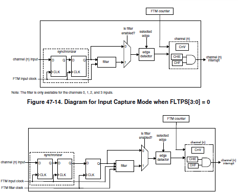
–> Input capture mode, the FlexTimer can measure the duty cycle or period of an input signal by detecting signal edges and generating interrupts. Here’s how it works:
- Edge Detection: When a signal edge (rising or falling) is detected on an FTM channel pin (e.g., FTM_CHx), the FTM copies its current counter (FTM_CNT) value into a capture register (FTM_CnV) and triggers an interrupt, if CHIE(Channel Interrupt Enabled) = 1.
- Interrupt Service Routine (ISR): In the ISR, you read the FTM_CnV value and store it in a variable. When the next edge occurs, the ISR runs again, and you save the new FTM_CnV value to another variable.
- Calculate Duty Cycle or Period:
- If edges are different (e.g., rising to falling), the difference between the two values gives the duty cycle.
- If edges are the same (e.g., rising to rising), the difference gives the signal period.
2. Edge-Aligned PWM Mode of FTM
–> Activation Conditions:
- DECAPEN = 0
- MCOMBINE = 0
- COMBINE = 0
- CPWMS = 0
- MSB = 1
–> In Edge-Aligned PWM Mode (EPWM), the period of the PWM signal is determined by the formula (MOD - CNTIN + 1), where MOD is the counter modulo value that sets the maximum counter value, and CNTIN is the initial counter value. The duty cycle, or the pulse width, is determined by either (CnV - CNTIN) or (MOD - CNTIN - CnV) depending on the settings of the ELSnB:ELSnA bits, which control the edge alignment. Here, CnV represents the channel value register that determines the time the output pin stays high, while CNTIN is the initial counter value and MOD is the maximum counter value. These formulas are crucial for setting the timing of the PWM signal and controlling the duration of its high state, thus defining the duty cycle and overall PWM behavior.

–> Special cases:
- CnV = 0x0000: Generates a 0% duty cycle, with CHF unset.
- CnV > MOD: Produces a 100% duty cycle if
MOD<0xFFFF.
–> With CNTIN ≠ 0, the PWM output range adjusts:
- CnV = CNTIN gives 0% duty.
- CNTIN < CnV ≤ MOD provides intermediate duty.
- CNTIN > CnV or CnV > MOD yields a 100% duty cycle.
3. Center-Aligned PWM Mode of FTM
- QUADEN = 0
- DECAPEN = 0
- MCOMBINE = 0
- COMBINE = 0
- CPWMS = 1
–> In Center-Aligned PWM Mode (CPWM), the PWM period is calculated as 2 × (MOD - CNTIN), where MOD is the maximum count value and CNTIN is the initial count value. The pulse width, or duty cycle, is determined by 2 × (CnV - CNTIN), where CnV(Channel Value) register defines the time the output pin stays high. The counter starts from CNTIN, counts up to MOD, then counts back down to CNTIN. During the down-count phase, an interrupt is generated when the counter matches CnV, signaling the start and end of the pulse width. This setup aligns the center of each pulse width across channels, creating a “center-aligned” PWM signal. For stability, MOD must be set within the range of 0x0001 to 0x7FFF.
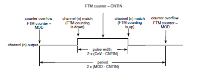
–> Channel Actions Based on ELSB
- 0:0: CHF set at match, output unchanged.
- 1:0: Output high (down count), low (up count).
- X:1: Output low (down count), high (up count).
–> Special Duty Cycles
- CnV = 0 or negative: 0% duty, CHF not set.
- CnV ≥ MOD: 100% duty, CHF not set.
4. Combine Mode of FTM
- QUADEN = 0
- DECAPEN = 0
- MCOMBINE = 0
- COMBINE = 1
- CPWMS = 0
–> In Combine Mode, two adjacent channels—an even-numbered channel (n) and the next odd-numbered channel (n+1)—are combined to generate a PWM signal on the output of the channel (n). The PWM period is calculated as (MOD - CNTIN + 1), where MOD is the maximum count and CNTIN is the initial count. The pulse width, or duty cycle, is determined by |C(n+1)V - C(n)V|, the absolute difference between the channel values for channels (n+1) and (n).
–> During the PWM cycle, when the FTM counter matches C(n)V, the channel (n) an interrupt is triggered (if enabled by setting CHIE). Similarly, the channel (n+1) interrupt triggers at the C(n+1)V match.
–> The ELSB:ELSA bits control the output behavior:
- If
ELSB:ELSA = 1:0for channel(n), the output is forced low at the start of the period(CNTIN)and at theC(n+1)Vmatch, but goes high at theC(n)Vmatch. - If
ELSB:ELSA = X:1for channel(n), the output is forced high at the start of the period, and theC(n+1)Vmatch, and goes low at theC(n)Vmatch.
- If
–> The ELSB:ELSA settings of channel (n+1) do not affect the combined output, except that if either channel’s ELSB:ELSA is set to 0:0, the output for that channel is no longer controlled by the FTM module.

5. Complementary Mode of FTM
–> In Complementary Mode, the output of channel (n+1) is the inverse of the output of channel (n), creating a complementary waveform. This mode is used to produce inverted PWM signals on two channels, which can be useful for driving complementary switches in power electronics.
However, Complementary Mode has some specific conditions:
Availability: It is not available in Output Compare mode.
Same Output Conditions: Channel
(n+1)will mirror the output of the channel(n)(i.e., it won’t be complimentary) when:QUADEN=0DECAPEN=0COMP=0- Channels
(n)and(n+1)are either in Combine Mode or Modified Combine PWM Mode.

Independent Output Conditions: Channel
(n+1)functions independently of the channel(n)when:QUADEN = 0DECAPEN = 0COMP = 0- Channel
(n)is in Output Compare mode, Edge-aligned PWM (EPWM), or Center-aligned PWM (CPWM).

4. PWM Synchronisation
–> PWM synchronization is a technique that allows real-time adjustments to the generated PWM signal directly from the microcontroller, enabling changes “on the fly.” Through synchronization, key buffered registers—such as MOD, HCR, CNTIN, CnV, OUTMASK, INVCTRL, and SWOCTRL—can be updated with pre-loaded values. These pre-loaded values of registers store buffered values that are applied during synchronization, allowing smoother PWM transitions. Various update schemes include software or hardware PWM synchronization, depending on the user requirements of the application.
A) Hardware Trigger in PWM Synchronisation
–> In PWM synchronization with hardware triggers, the FTM module uses three hardware trigger inputs (TRIG0, TRIG1, and TRIG2), which activate when their respective TRIGn bit is set to 1. Each trigger is synced to the FTM input clock, initiating PWM synchronization on a rising edge at an enabled hardware trigger input.
- If HWTRIGMODE is set to 0, the TRIGn bit clears either when 0 is written to it or when a trigger event occurs. Notably, if multiple triggers are enabled (e.g., TRIG0 and TRIG1 are set to 1) but only trigger 1 fires, then only TRIG1 clears. If a trigger event and a write operation happen simultaneously, synchronization still starts, but the TRIGn bit stays set due to the write.
- If HWTRIGMODE is set to 1, the TRIGn bit only clears when 0 is explicitly written to it. This mode is compatible only with enhanced PWM synchronization (when SYNCMODE is set to 1), ensuring that hardware triggers function correctly with synchronized updates in enhanced PWM applications
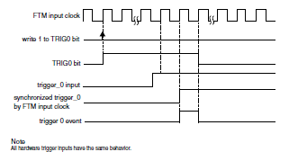
B) Software Trigger in PWM Synchronisation
–> A software trigger event occurs when a 1 is written to the SYNC[SWSYNC] bit. The SWSYNC bit then clears either when 0 is written to it or once the PWM synchronization from that software event completes. If another software trigger event is initiated (by writing 1 to SWSYNC) as the prior synchronization is ending, a new PWM synchronization starts, and SWSYNC remains 1.
If SYNCMODE = 0, the SWSYNC bit also clears according to the PWMSYNC and REINIT bits. Specifically:
- If PWMSYNC = 1, or PWMSYNC = 0 and REINIT = 0, the SWSYNC bit clears at the next selected loading point after the software trigger.
- If PWMSYNC = 0 and REINIT = 1, it clears immediately when the software trigger occurs.
If SYNCMODE = 1, SWSYNC clears based on the SWRSTCNT bit:
- If SWRSTCNT = 0, SWSYNC clears at the next loading point after the software trigger.
- If SWRSTCNT = 1, SWSYNC clears immediately when the software trigger event happens.
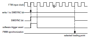
5. Global Time Base (GTB)
–> The Global Time Base (GTB) mechanism on S32K devices enables synchronization across multiple independent FTM modules when more PWM channels are needed than a single FTM can offer(like each FTM module offers 8 channels but I want to use 12 channels with same configuration). By keeping counters aligned across FTMs, GTB acts as a synchronous signal from a master FTM, ensuring all FTM counters begin counting together under the same clock source and at the same time.
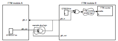
–> GTB configuration uses GTBEEN and GTBEOUT bits in the CONF register:
- GTBEEN = 1 allows gtb_in to control the FTM counter enable signal.
- GTBEEN = 0 allows each FTM module to function independently.
–> The gtb_in and gtb_out signals interconnect FTMs, enabling their counters to operate synchronously as a unified time base, giving the appearance of a single module with synchronized PWM channels. However, GTB only synchronizes the start of counting—counters may lose synchronization during extended operation.
Enabling the Global Time Base (GTB)
–> To enable the Global Time Base (GTB) feature for synchronized PWM across multiple FTM modules, follow these steps for each participating module:
- Stop the FTM Counter: Set
SC[CLKS]to00b. - Configure the FTM Module: Set up the FTM module with consistent settings across all participating FTMs.
- Enable GTB: Set
CONF[GTBEEN]to1andCONF[GTBEOUT]to0simultaneously. - Select a Clock Source: Choose the same clock source for each module by setting
SC[CLKS]. - Reset the FTM Counter: Write any value to the
CNTregister.
- Stop the FTM Counter: Set
–> To activate GTB synchronization, set CONF[GTBEOUT] to 1 in the designated master FTM module, which will serve as the time base for other modules.
FTM-PERIPHERAL REGISTER
- In this section, we’ll match the above learning features of the FTM Peripheral with Microcontroller Registers.
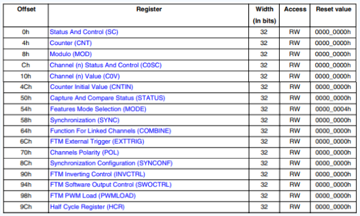
- Above mentioned image demonstrates all the active registers in the FTM peripheral. But our main focus of interest is SC, CNT, MOD, CnSC, CnV, CNTIN, STATUS, MODE, SYNC, COMBINE, EXTTRIG, POL, SYNCONF, INVCTRL, SWOCRTL, PWMLOAD and HCR registers. This contains our learned feature of the FTM Peripheral.
